<< Chapter < Page Chapter >> Page >
Figure five contains two parts. Part a, titled Block Diagram of a Synchronous Digital Resampler, is a flowchart. Beginning from the left, a caption reads x(k) @f_in 8 kHz. An arrow points to the right at a circle containing a large x. Below the circle is a box with the label, Digital Local Oscillator. An arrow from this box points up at the circle. Next to this arrow is the expression e^-jωkT. To the right of the circle is an arrow pointing to the right at another box, labeled Zero-fill by 12. To the right of this box is an arrow pointing to the right, and below this arrow is the expression 12⋅F_in = 96 kHz. The arrow points to the right at a box labeled FIR Digital Lowpass Filter. Another arrow pointing to the right follows, with the expression below, 12 ⋅ f_in = 96 kHz. The arrow points at a box labeled Decimate by 25. This is followed by a final arrow pointing to the right. Above the arrow is the expression z(r), and below the arrow is the expression f_out = f_in ⋅ 12/25 = 3840 Hz. Part b is a photograph of a tuner card with its width measured as the length of a ruler.
The Use of a Resampling Tuner to Provide the Inputs to FSK VFT Demodulator "Filter Bank" Card

Asic-based implementation of fdm group tuning and transmultiplexing

A number of apparently inoffensive assumptions were made in the development of the tradeoff formulas used in the previous examples. One was that one-step (also called single stage ) decimation is used in the tuner's filtering and the other is that the number of multiplications and additions forms good basis for comparing the complexity of various designs. This example demonstrates some counterexamples along the way to the description of a system that represents the current state of the art (circa 1990) in tuner and transmultiplexer design.

Suppose that our goal is to accept a full 2700-channel FDM telephone baseband, select an FDM group with a tuner, and then demultiplex the constituent 12 voice grade channels with a transmultiplexer. In the now-familiar way, we develop the certain specifications for the transmultiplexer and tuner separately and then jointly optimize the shared parameters.

  • Transmultiplexer: To achieve the desired channel shaping, we select Q to be 16. To minimize the amount of computation, we set K to unity. The window/tuner pulse response chosen provides an adjacent channel rejection of better than 55 dB and an NPR of about 55 dB.
  • Tuner: A 2700-channel baseband extends up to 12388 kHz. Leaving a transition band for an analog antialias filter and looking for a power of two times 4 kHz leads to the selection of 32768 kHz as f i n , the baseband digitization rate. The tuner output bandwidth B t must be at least 48 kHz to pass an FDM group. Owing the high tuner decimation required, we assume that α t must be on the order of 3.

We now turn to [link] to determine the optimum value of f s , and with it, M t , L t , and N . Plugging in to this equation yields an optimal f s of about 490 kHz, more than ten times greater than the FDM group's bandwidth. In analyzing this result, we find that the amount of computation needed by a single-step FIR decimating tuner is so high that it dominates that needed by the transmultiplexer. Clearly another approach is needed.

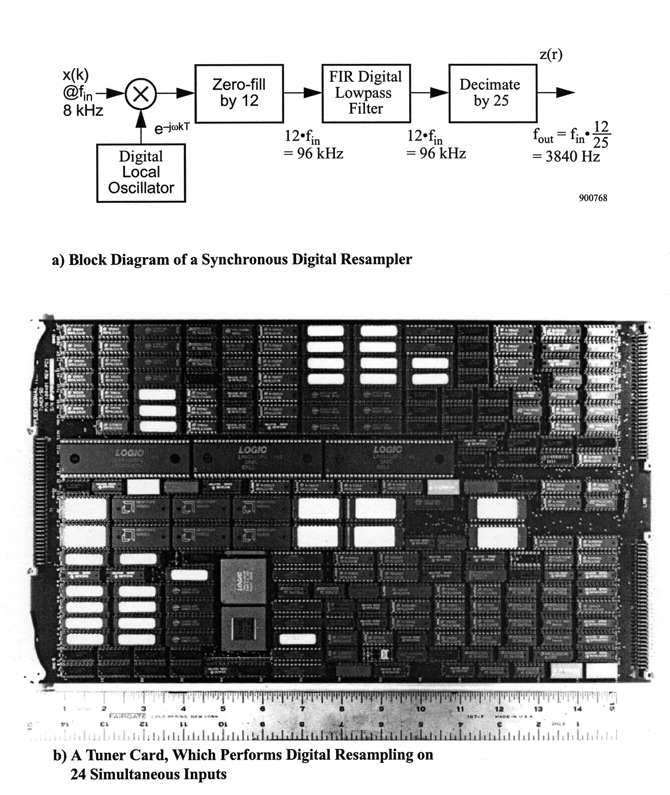
In response to this problem, the company developed a pair of custom application-specific ICs (ASICs) for selecting FDM groups from digitized basebands and another chip for transmultiplexing four FDM groups. The block diagram is essentially the same as that shown in Figure 1 from "Derivation of the equations for a Basic FDM-TDM Transmux" except that a multistage decimating filter is used. In all, nine filter stages are employed. Each bandlimits the incoming signal sufficiently that a decimation by two is possible. The first few stages, the ones that must operate at very high rates, use pulse responses so simple (for example, h ( k ) = [ 1 , 2 , 1 ] ) that only shifting and addition are needed. The effect of nine divisions by 2 is the reduction of the sampling rate f s to 64 kHz. The 48-kHz-wide FDM group is thus represented at the output of the tuner chips as complex-valued samples at a rate of 64 kHz.

The transmultiplexer ASIC accepted four FDM groups, each quadrature-sampled at 64 kHz, and demultiplexes all 48 voice grade channels. A block diagram of a single path through the device is shown in [link] . The window-and-fold circuit was implemented by using onboard weighting coefficients and serial multipliers. The partial sums were stored in off-chip RAM. The output of the window-and-fold circuit was then transformed using a 16-point DFT. The complex-valued bin outputs, produced at a 4 kHz rate, were sent out over a serial interface.

Figure six is a complex flow chart. Two rows begin the flow, the top labeled I and the bottom labeled Q. A line extends to the right with a hash mark in the middle numbered as 1. The line extends to two rectangles, both labeled NIBEXT. An arrow on the right side of these rectangles points to the left. Above the middle of these arrows is a single rectangle, labeled Ext RAM 8k x 8, and two arrows that point in both directions extend down to the two lines below. In the middle of these two arrows are hash marks that are numbered with a 4. To the right of the arrows that point to the left are two rectangles labeled Word EXT. After this point, to the right, is a large dashed box labeled WF that encapsulates the next handful of objects. Lines extend to the right from the Word EXT boxes, with hash marks numbered as 16. These lines connect to two circles containing a large x. A multi-directional arrow connects these two circles together, and from the middle of this arrow extends a line downward. This line includes a hash mark numbered 16, and it connects to a box below containing the label WF Coef ROM. Below this rectangle is the caption 512 x 16. To the right of the x-circles is a line containing hash marks numbered as 32. These lines connect to two more circles containing a large plus sign. A line from the right side of these circles extends horizontally, and contains the hash mark numbered 16. In the middle of these lines are an arrow that points upward, to the right, and back down to the top of the circles with plus signs. This is the end of the WF section. The lines with the hash marks numbered 16 extend to the right and connect to a single large rectangle, labeled Dual Port 32 x 32. To the right of the large rectangle are two lines that include hash marks numbered 16. Across these lines is a second large dashed rectangular box, titled DFT, that encapsulates the next handful of objects. Out of the two 16-hash marks, the hash mark  on the top line occurs before the line enters the DFT box, and the bottom occurs inside the DFT box. These lines connect to two more circles that contain a large x, aligned with those below them from top to bottom. Along these lines before the circles, there are extension lines above and below to various other segments of the graph. First, two arrows from the middle of these lines point upward, then to the right, at two more circles containing a large x. Below the lines, towards the bottom of this portion of the figure in the DFT box are two boxes labeled Cos ROM, 16 x 16, and Sine ROM, 16 x 16. From the Cos box, a line extends upward to the upper-most x-circle, and a line extends to the lowest x-circle. From the Sine box, a line extends up to a set of arrows that connect the two middle x-circles, one from the original group, and one from the group situated above. The upper circles both point at a single circle to the right containing a - sign. This is connected with a short line to another circle, containing a + sign. A line extends to the right after this circle, and points outside the DFT box to a rectangle. The rectangle contains a P, a short arrow pointing to the right, and an S. On the line in between the circle with the plus sign and the rectangle, there is a line segment that points up, to the left, and back down to the top of the circle. This line contains a hash mark numbered 32. To the right of the rectangle on the rightmost part of the flow chart is a final arrow pointing at a label I. The arrow contains a hash mark numbered with a 1. The lower x-circles follow a similar flow, except the + sign circle precedes the - sign circle. The P S rectangle is the same, but the arrow pointing to the right points at the caption Q. Also, an arrow from the line in between the circles and the P S rectangle  extends downward and to the right at a final rectangle, labeled Power Meas, which continues with an arrow to the right that points at the caption P.
Block Diagram of a Quad Group Transmux ASIC

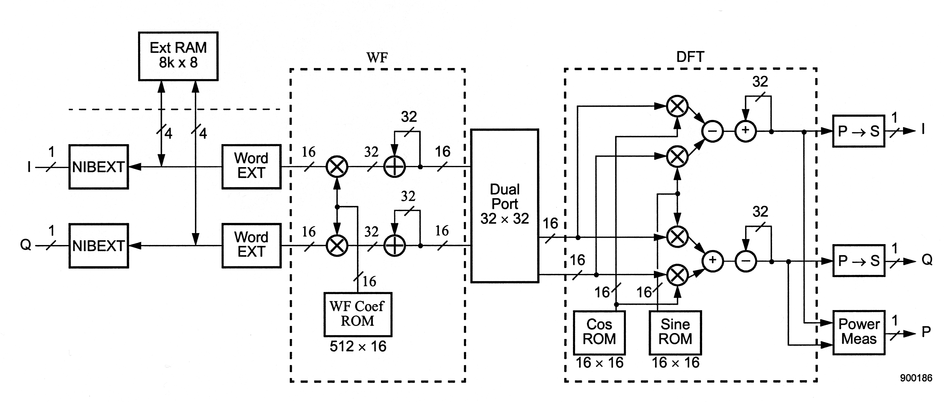
Several of the design choices made with these chips are different that those seen earlier in the technical note. The first, seen in the tuner chips, is the use of multistage decimation. As [link] shows, this can almost always reduce the total amount of multiply-add computation needed for the tuner, at a certain cost in design simplicity. The other issue, evident in the design of both the tuner and the transmultiplexer, is that memory and control are at least as costly commodities in an ASIC design as are multiplications and additions. A vivid example is that the transmux ASIC used direct computation of the DFT rather than using an FFT. Even though the amount of multiplication is on the order of four times as much using the DFT, the overall DFT design used less silicon than the equivalent FFT.

Get Jobilize Job Search Mobile App in your pocket Now!

Get it on Google Play Download on the App Store Now


Source:  OpenStax, An introduction to the fdm-tdm digital transmultiplexer. OpenStax CNX. Nov 16, 2010 Download for free at http://cnx.org/content/col11165/1.2
Google Play and the Google Play logo are trademarks of Google Inc.

Notification Switch

Would you like to follow the 'An introduction to the fdm-tdm digital transmultiplexer' conversation and receive update notifications?

Ask