

| << Chapter < Page | Chapter >> Page > |
Actually, implants (especially for moats) are usually done at a sufficiently high energy so that the dopant(phosphorus) is already pretty far into the substrate (often several microns or so), even before the diffusion starts. Theanneal/diffusion moves the impurities into the wafer a bit more, and as we shall see also makes the n-region grow larger.
"The n-region"! We have not said a thing about how we make our moat in only certain areas of the wafer. Fromthe description we have so far, is seems we have simply built an n-type layer over the whole surface of the wafer. This would bebad! We need to come up with some kind of "window" to only permit the implanting impurities to enter the silicon waferwhere we want them and not elsewhere. We will do this by constructing an implantation "barrier".
To do this, the first thing we do is grow a layer of silicon dioxide over the entire surface of the wafer. Wetalked about oxide growth when we were discussing MOSFETs but let's go into a little more detail. You can grow oxide in eithera dry oxygen atmosphere, or in a an atmosphere which contains water vapor, or steam. In [link] , we show oxide thickness as a function of time for growth with steam. Dry O 2 does not behave too much differently, the rate is just somewhat slower.

On top of the oxide, we are now going to deposit yet another material. This is silicon nitride, Si 3 N 4 or just plain "nitride" as it is usually called. Silicon nitride is deposited through a method calledchemical vapor deposition or "CVD". The usual technique is to react dichlorosilane and ammonia in a hot walled low pressurechemical vapor deposition system (LPCVD). The reaction is:
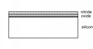
Silicon nitride is a good barrier for impurities, oxygen and other things which do not want to get into the wafer. Take alook at [link] and see what we have so far. A word about scale and dimensions. The silicon wafer is about250 μm thick (about 0.01") since it has to be strong enough not to break as it is being handled. The two deposited layersare each about 1 μm thick, so they should actually be drawn as lines thinner than the other lines in the figure. This wouldobviously make the whole idea of a sketch ridiculous, so we will leave things distorted as they are, keeping in mind that thedeposited and diffused layers are actually much thinner than the rest of wafer, whichreally does not do anything except support the active circuits up on top.
Now what we want to do is remove part of the nitride, so we can make our n-well, but not put inphosphorous where do not want it. We do this with a processes called photolithography and etching respectively. First thing we do is coat the wafer with yetanother layer of material. This is a liquid called photoresist and it is applied through a processcalled spin-coating. The wafer is put on a vacuum chuck, and a layer of liquid photoresist is sprayed uncap of thewafer. The chuck is then spun rapidly, getting to several thousand RPM in a small fraction of a second. Centrifugal forcecauses the resist to spread out uniformly across the wafer surface. The solvent for thephotoresist is quite volatile and so the layer of photoresist dries while the wafer is still spinning, resulting in a thin,uniform coating across the wafer [link] .
Notification Switch
Would you like to follow the 'Chemistry of electronic materials' conversation and receive update notifications?

|
|

|
|

|
|

|
|

|
|

|
|

|
|

|
|
|
|
|

|