

| << Chapter < Page | Chapter >> Page > |

The name "photoresist" gives some clue as to what this stuff is. Basically, photoresist is a polymer mixed with some kind oflight sensitizing compound. In positive photoresist, wherever light strikes it, the polymer is weakened,and it can be more easily removed with a solvent during the development process. Conversely,negative photoresist is strengthened whenit is illuminated with light, and is more resistant to the solvent than is the unilluminated photoresist. Positive resistis so-called because the image of the developed photoresist on the wafer looks just like the mask that was used to createit. Negative photoresist makes an image which is the opposite of what the mask looks like.
We have to come up with some way of selectively illuminating certain portions of the photoresist. Anyone who hasever seen a projector know how we can do this. But, since we want to make small things, not big ones, wewill change around our projector so that it makes a smaller image, instead of a bigger one. The instrument that projects thelight onto the photoresist on the wafer is called a projection printer or stepper [link] .

As shown in [link] , the stepper consists of several parts. There is a light source (usually a mercury vaporlamp, although ultra-violet excimer lasers are also starting to come into use), a condenser lens to image the light source onthe mask or reticle. The mask contains an image of the pattern we are trying the place onthe wafer. The projection lens then makes a reduced (usually 5x) image of the mask on the wafer. Because it would be far toocostly, if not just plain impossible, to project onto the whole wafer all at once, only a small selected area is printed at onetime. Then the wafer is scanned or stepped into a new position, and the image isprinted again. If previous patterns have already been formed on the wafer, TV cameras, with artificial intelligence algorithmsare used to align the current image with the previously formed features. The stepper moves the whole surfaceof the wafer under the lens, until the wafer is completely covered with the desired pattern. A stepper is one of the most important pieces ofequipment in the whole IC fab however, since it determines what the minimum feature size on the circuit will be.
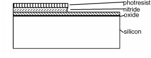
After exposure, the photoresist is placed in a suitable solvent, and "developed". Suppose for our example thestructure shown in [link] is what results from the photolithographic step.

The pattern that was used in the photolithographic (PL) step exposed half of our area to light, and so the photoresist (PR)in that region was removed upon development. The wafer is now immersed in a hydrofluoric acid (HF) solution. HF acid etchessilicon nitride quite rapidly, but does not etch silicon dioxide nearly as fast, so after the etch we have what we see in [link] .
We now take our wafer, put it in the ion implanter and subject it to a "blast" of phosphorus ions [link] .

The ions go right through the oxide layer on the RHS, but stick in the resist/nitride layer on the LHS of our structure.
Notification Switch
Would you like to follow the 'Chemistry of electronic materials' conversation and receive update notifications?

|
|

|
|

|
|

|
|

|
|
|
|
|

|
|

|
|

|
|

|