

| << Chapter < Page | Chapter >> Page > |
SSPD_Chapter 7_Part 3_Basic Electrical Properties of MOSFET_continued7
7.3.14. Comparative aspects of Key Parameters of CMOS and BJT.
In the Table 7.3.14.1 we enumerate the major differences of CMOS and BJT in qualitative terms then we will deal with it in quantitative terms.
Table 7.3.14.1. Comparative study of CMOS and BJT.
| Bipolar Junction Transistors | CMOS | |
| Carriers involved in transistor action | Bipolar(both minority and majority cariers are involved) | Unipolar (only majority carriers participate) |
| Input dynamic range | Exponential device hence input dynamic range for linear applications is 5mV | Quadratic Device hence input dynamic range for linear applications is 400mV |
| Noise Figure | Much higher hence not suitable for Low Noise Amplifier | At cryogenic temperatures its Noise Figure is nearly Unity hence MESFET is suitable for LNA |
| Packing Density | Because of isolation diffusion BJT ICs are traditionally 1-G behind in level of integration. | This has far ahead in packing density. |
| Speed | Historically it is much faster because transit through base width limits the switching speed. It has reached more than 100GHz | Here the transit through the channel length limits the speed. The maximum switching speed is 2GHz or more. |
| Transconductance | 40mS at 1mA | 1mS at 1mA |
| Drive capability(A/cm 2 ) | 10 times more than that of CMOSHence at the driver stage we use BiCMOS |
7.3.14.1. Quantitative analysis of the key parameters of BJT and CMOS.
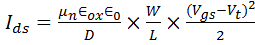
In the Pentode region of operation:


Therefore:

Where

In circuit application books β is referred to as K n , transcoductance parameter for NMNOS.
Substituting the values of the different parameters in Eq.7.3.12.4 we get:


Therefore β = (W/L)×69(µA/V 2 )
In Table 7.3.14.2 we get the special transconductance parameter for different aspect ratio.
Table 7.3.14.2. Special Transconductance Parameter for different geometries.
| W | L | W/L | β(µA/V 2 ) |
| 20µm | 1 µm | 20 | 1380 |
| 60 µm | 3 µm | 20 | 1380 |
| 10 µm | 0.25 µm | 40 | 2760 |
From Section 7.3.5 we get:


Where

Dividing Eq.7.3.23 by 7.3.12.3 we get:

We will choose W/L = 10µm/0.25µm = 40.
Special transconductance parameter = β= 40×69µA/V 2 = 2760 µA/V 2
Therefore:

Then V GS -V Tn =0.851V.
Substituting this value in Eq.7.3.14.1
We get :

Similarly if we analyze BJT we get :


I C = d.c. collector current and V t = thermal voltage = kT/q = 25mV at 300K_Room Temperature.

By comparing Eq 7.3.14.2 aand 7.3.14.4 we see that for same bias current 1mA, BJT delivers 17 times transconductace as compared to that of MOSFET.
7.3.14.2. Current Delivery Capability of BJT and MOSFET.
Rewriting Eq.7.3.12.3

Where

Therefore:
Or

Calculating for W/L = 10µm/0.25µm = 40. And D = 25nm we get:

Analyzing for I DS = 1mA we get:

Expressing it in A/cm 2 we get:

7.3.14.2.1. Current delivery capability of BJT.
From the Physics of BJT we have the following relationship:

Therefore:

Where W B = effective base width, n po = thermal equilibrium value of minority carrier in Base; λ = Exp(V BE /V t ).
From Device Physics we also know that the Collector Current is diffusion current given by the following expression:

Since our reference current is I C = 1mA and we choose A E = 1(µm) 2
Therefore

Therefore

Therefore

Following are the various parameter values:q=1.6×10 -19 Coulombs, µ n = bulk electron mobility=1450 cm 2 /(V-sec), Thermal Voltage= V thermal = kT/q =25mV at 300Kelvin, n po = thermal equilibrium value of minority carriers in Base in a NPN transistor = 10 3 /cm 3 and W B = effective base width = 1µm=1×10 -4 cm.
Substituing the above values in Eq.7.3.14.12 we get:

By inspection we see that it is a dimensionless quantity therefore:

We substitute the value of λ=1.724×10 15 in Eq.7.3.14.10:

Eq.7.3.14.13 is dimensionally balanced.

Comparing Eq 7.3.14.8 and Eq.7.3.14.14 we see that BJT has 10 times drive capability.
7.3.14.3.Quantitative differences in the key parameters
| BIPOLAR TRANSISTOR | MOSFET | |
| Current drive capability for 1mA in units of A/cm 2 | 4,31,000 | 40,000 |
| Transconductance/Bias Current(1/V) | 40 | 2.35 |
| Transconductace(Siemens) | Varies directly as bias current | Varies as the square root of the bias current |
| Transconductance as a function of geometry | Weak function | Strongly dependent on aspect ratio and oxide thickness |
| Transconductance as a function of process technology | Independent | Dependent through oxide thickness |
Notification Switch
Would you like to follow the 'Solid state physics and devices-the harbinger of third wave of civilization' conversation and receive update notifications?

|
|

|
|

|
|

|
|

|
|
|
|
|

|
|

|
|

|
|

|