

| << Chapter < Page | Chapter >> Page > |
SSPD_Chapter 7_Part 3_Basic Electric Properties of MOSFET_Continued_8
7.3.15. BiCMOS Inverters.

In the output stage where loads have to be driven, CMOS Logic Gates themselves cannot give adequate current for drivng the loads. In these circuits buffer BJT are added as shown in Figure 7.3.15.1. The inverted logic operation is carried out as shown in Table 7.3.15.1.
Table 7.3.15.1. The Inverted Logic Operation of BiCMOS inverter.
| Input | Q1 | Q2 | Q3 | Q4 | Vout |
| LOW(GND) | off | On and Q2 sources current to charge C L to 5V through a low impedance path provided by on BJT Q2 | off | on | HIGH=5-V BE (on) |
| HIGH(5V) | On and Q1 sinks current thereby discharging C L through low impedance path provided by on BJT Q1 | off | on | off | LOW = V CE (sat) |
The characteristics of BiCMOS Inverter.
i.Logic levels are close to bus voltages;
ii.High input impedance;
iii.Low output impedance;
iv. It has high current drive capability and occupies a relatively small area;
v. It has large Noise Margin.
But this configuration has high standby dissipation under I/P = HIGH condition since Q1 and Q3 provide a low impedance path from Positive Bus to GND bus.
Also this configuration has no path for turning off the BJT when required.This slows the switching operation. Hence we go for improved circuit configuration.

In Figure 7.3.15.2 we have removed the direct dc path from Positive Bus to GND through Q3 and Q1 but when Vin = HIGH, Vout ≠ V CE (sat) which is 0.2V but Vout = V BE (on) = 0.7V. Hence output swing is reduced from full 5V to about 4V.
Also BJTs still donot have a discharge path for their base currents during turn off of the respective BJT. So a third configuration is given in Figure 7.3.15.3.
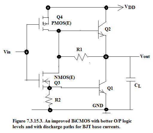
In the improved version shown in Figure 7.3.15.3. two resistances R1 and R2 are introduced in the discharge paths of the bases of the BJTs , Q1 and Q2. Because of the resistances, the logic levels are improved and hence voltage swing is optimized. The resistances also speed up the switching of the transistors.
Though this is an improved version of BiCMOS Inverter from IC technology point of view it is impractical because passive chip resistances occupy large real estate area and suitable values are difficult to realize. Hence chip resistances are replaced by MOS transistors as shown in Figure 7.3.15.4.
In Figure 7.3.15.4, the function of R1 is fulfilled by Q5 and function of R2 is fulfilled by Q6. The states of different transistors during Inverted Logic Operation are given in Table 7.3.15.2.
Table 7.3.15.2. Inverted Logic Operation of the optimized version ogf BiCMOS.
| Vin | Q1 | Q2 | Q3 | Q4 | Q5 | Q6 | Vout |
| HIGH | SAT | OFF | ON | OFF | ONThis provides the discharge path for the base current of Q2 which was ON previously | OFF | LOW=V CE (sat) |
| LOW | OFF | ON | OFF | ON | OFF | ONThis provides the discharge path for the base current of Q1 which was in SAT previously | HIGH |

This circuit offers enormous advantages where high load current sourcing and sinking are required. Whenever Video Monitors or Speakers are to be driven there we require BiCMOS interface at the output.
Notification Switch
Would you like to follow the 'Solid state physics and devices-the harbinger of third wave of civilization' conversation and receive update notifications?

|
|

|
|

|
|

|
|
|
|
|

|
|

|
|

|
|

|
|

|