

| << Chapter < Page | Chapter >> Page > |
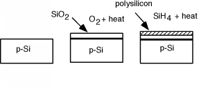
[link] shows the basic steps necessary to make the MOS structure. It will help us in our understanding if we now rotateour picture so that it is pointing sideways in our next few drawings. [link] shows the rotated structure. Note that in the p-silicon we have positively chargedmobile holes, and negatively charged, fixed acceptors. Because we will need it later, we have also shown the band diagram forthe semiconductor below the sketch of the device. Note that since the substrate is p-type, the Fermi level is located downclose to the valance band.
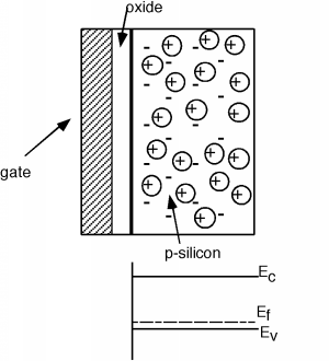
Let us now place a potential between the gate and the silicon substrate. Suppose we make the gate negative with respect to thesubstrate. Since the substrate is p-type, it has a lot of mobile, positively charged holes in it. Some of them will beattracted to the negative charge on the gate, and move over to the surface of the substrate. This is also reflected in the banddiagram shown in [link] . Remember that the density of holes is exponentially proportional to how close the Fermi level is tothe valence band edge. We see that the band diagram has been bent up slightly near the surface to reflect the extra holeswhich have accumulated there.

An electric field will develop between the positive holes and the negative gate charge. Note that the gate and the substrateform a kind of parallel plate capacitor, with the oxide acting as the insulating layer in-between them. The oxide is quite thincompared to the area of the device, and so it is quite appropriate to assume that the electric field inside the oxideis a uniform one. (We will ignore fringing at the edges.) The integral of the electric field is just the applied gate voltage V g . If the oxide has a thickness x ox then since E ox is uniform, it is given by, [link] .
If we focus in on a small part of the gate, we can make a little "pill" box which extends from somewhere in the oxide, across theoxide/gate interface and ends up inside the gate material someplace. The pill-box will have an area Δ s . Now we will invoke Gauss' law which we reviewed earlier. Gauss' law simply says that the surface integral over aclosed surface of the displacement vector D (which is, of course, ε x E ) is equal to the total charge enclosed by that surface. We will assume that there is a surfacecharge density -Q g Coulombs/cm 2 on the surface of the gate electrode ( [link] ). The integral form of Gauss' Law is just:

Note that we have used ε ox E in place of D . In this particular set-up the integral is easy to perform, since theelectric field is uniform, and only pointing in through one surface - it terminates on the negative surface charge insidethe pill-box. The charge enclosed in the pill box is just -( Qg Δ s ), and so we have (keeping in mind that the surface integral of a vectorpointing into the surface is negative), [link] , or [link] .
Notification Switch
Would you like to follow the 'Chemistry of electronic materials' conversation and receive update notifications?

|
|

|
|
|
|
|

|
|

|
|
|
|
|

|
|
|
|
|

|
|

|