

| << Chapter < Page | Chapter >> Page > |
Now, we can use [link] to get [link] or [link] .
The quantity c ox is called the oxide capacitance. It has units of Farads/cm 2 , so it is really a capacitance per unit area of the oxide. The dielectric constant of silicondioxide, ε ox , is about 3.3 x 10 -13 F/cm. A typical oxide thickness might be 250 Å (or 2.5 x 10 -6 cm). In this case, c ox would be about 1.30 x 10 -7 F/cm 2 . The units we are using here, while they might seem a little arbitrary and confusing, are the ones most commonly usedin the semiconductor business.
The most useful form of [link] is when it is turned around, [link] , as it gives us a way to find the charge on the gate in terms of the gate potential. We will use this equation later in our development ofhow the MOS transistor really works.
It turns out we have not done anything very useful by apply a negative voltage to the gate. We have drawn more holes there inwhat is called an accumulation layer, but that is not helping us in our effort to create a layer of electrons inthe MOSFET which could electrically connect the two n-regions together.
Let's turn the battery around and apply a positive voltage to the gate ( [link] ). Actually, let's take the battery out for now, and just let V g be a positive value, relative to the substrate which will tie to ground. Making V g positive puts positive Q g on the gate. The positive charge pushes the holes away from the region under the gate anduncovers some of the negatively-charged fixed acceptors. Now the electric field points the other way, and goes from the positivegate charge, terminating on the negative acceptor charge within the silicon.
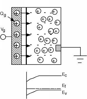
The electric field now extends into the semiconductor. We know from our experience with the p-n junctionthat when there is an electric field, there is a shift in potential, which is represented in the band diagram by bendingthe bands. Bending the bands down (as we should moving towards positive charge) causes the valence band to pull away from theFermi level near the surface of the semiconductor. If you remember the expression we had for the density of holes in termsof E v and E f it is easy to see that indeed, [link] , there is a depletion region (region with almost no holes) near the region under the gate. (Once E f - E v gets large with respect to kT , the negative exponent causes .)
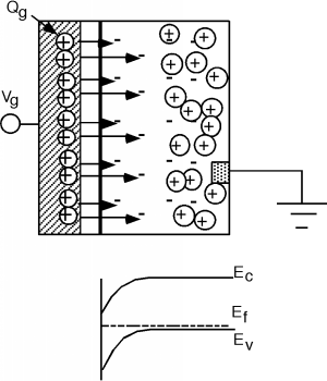
The electric field extends further into the semiconductor, as more negative charge is uncovered and the bands bend furtherdown. But now we have to recall the electron density equation, which tells us how manyelectrons we have:
A glance at [link] reveals that with this much band bending, E c the conduction band edge, and E f the Fermi level are starting to get close to one another (at least compared to kT ), which means that n , the electron concentration, should soon start to become significant. In the situation represented by [link] , we say we are at threshold , and the gate voltage at this point is called the threshold voltage , V T .
Now, let's increase V g above V T . Here's the sketch in [link] . Even though we have increased V g beyond the threshold voltage, V T , and more positive charge appears on the gate, the depletion region no longer moves back into thesubstrate. Instead electrons start to appear under the gate region, and the additional electric field lines terminate onthese new electrons, instead of on additional acceptors. We have created an inversion layer of electrons under the gate, and it is this layer of electrons which we can use toconnect the two n-type regions in our initial device.
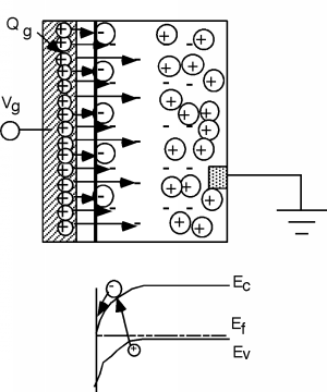
Where did these electrons come from? We do not have any donors in this material, so they can not come from there. The onlyplace from which electrons could be found would be through thermal generation. Remember, in a semiconductor, there arealways a few electron hole pairs being generated by thermal excitation at any given time. Electrons that get created in thedepletion region are caught by the electric field and are swept over to the edge by the gate. I have tried to suggest this withthe electron generation event shown in the band diagram in the figure. In a real MOS device, we have thetwo n-regions, and it is easy for electrons from one or both to "fall" into the potential well under the gate, and create theinversion layer of electrons.
Notification Switch
Would you like to follow the 'Chemistry of electronic materials' conversation and receive update notifications?

|
|

|
|

|
|

|
|

|
|

|
|

|
|

|
|

|
|

|