<< Chapter < Page Chapter >> Page >
This module gives a brief general overview of semi-conductor manufacturing and some of the components and processes used to produce them that can potentially cause harm to humans or the environment.
"This module was developed as part of a Rice University Class called " Nanotechnology: Content and Context "initially funded by the National Science Foundation under Grant No. EEC-0407237. It was conceived, researched, written and edited by students in the Fall 2005 version of the class, and reviewed by participating professors."

What is a semiconductor?

The semiconductor industry is one of the fastest growing manufacturing sectors in not only the United Statesbut also in the world. According to the American Electronics Association, the domestic sales of electronic components haveskyrocketed, jumping from $127 billion to $306 billion over the course of the 1980’s. In the first three quarters of the 2003fiscal year alone, the export of technology goods from the United States increased by $19 billion [1].

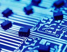
The word “semiconductor” technically refers to any member of a class of solid, crystalline materials that ischaracterized by an electrical conductivity better than that of insulators (e.g., plastic) but less than that of good conductors(e.g., copper) [2]. Semiconductors are particularly usefulas a base material in the manufacturing of computer chips, and the term semiconductor has actually come to be synonymous with thecomputer chips, themselves. However, semiconductors are not only used in computers. Computers only make up 44% of entire industryconsumption (see [link] ). Semiconductors are also used for military, automotive, industrial, communications, and other consumer purposes.

Relative consumption of semiconductors by industry [3].

Semiconductors seem to be anywhere and everywhere throughout our everyday lives, yet it is surprising howlittle most people know about how they actually work or about the potentially devastating effects their manufacturing can have on theenvironment and human health.

Why is nanotechnology important to the semiconductor industry?

Much of the study of nanotechnology has been centered on the manufacturing of semiconductors. Though there are a number of highly anticipated applications for nanotechnology in other fields,notably in medicine and in biotechnology, the most tangible results thus far can be argued to have been achieved in the semiconductorindustry.

An example of a semiconductor (photo from PEAK).

For example, Intel recently unveiled its first products based on a generation of 90-nanometer processtechnology, and its researches and engineers have built and tested prototype transistors all the way down to the 22-nanometer range.Currently, Intel scientists and engineers are working on identifying new materials such as carbon nanotubes and nanowires toreplace current transistors, and in particular they hope to develop a “tri-gate” transistor approach that would enable chip designersto build transistors below the 22-nanometer range [4].

Questions & Answers

what is phylogeny
Odigie Reply
evolutionary history and relationship of an organism or group of organisms
AI-Robot
ok
Deng
what is biology
Hajah Reply
the study of living organisms and their interactions with one another and their environments
AI-Robot
what is biology
Victoria Reply
HOW CAN MAN ORGAN FUNCTION
Alfred Reply
the diagram of the digestive system
Assiatu Reply
allimentary cannel
Ogenrwot
How does twins formed
William Reply
They formed in two ways first when one sperm and one egg are splited by mitosis or two sperm and two eggs join together
Oluwatobi
what is genetics
Josephine Reply
Genetics is the study of heredity
Misack
how does twins formed?
Misack
What is manual
Hassan Reply
discuss biological phenomenon and provide pieces of evidence to show that it was responsible for the formation of eukaryotic organelles
Joseph Reply
what is biology
Yousuf Reply
the study of living organisms and their interactions with one another and their environment.
Wine
discuss the biological phenomenon and provide pieces of evidence to show that it was responsible for the formation of eukaryotic organelles in an essay form
Joseph Reply
what is the blood cells
Shaker Reply
list any five characteristics of the blood cells
Shaker
lack electricity and its more savely than electronic microscope because its naturally by using of light
Abdullahi Reply
advantage of electronic microscope is easily and clearly while disadvantage is dangerous because its electronic. advantage of light microscope is savely and naturally by sun while disadvantage is not easily,means its not sharp and not clear
Abdullahi
cell theory state that every organisms composed of one or more cell,cell is the basic unit of life
Abdullahi
is like gone fail us
DENG
cells is the basic structure and functions of all living things
Ramadan
What is classification
ISCONT Reply
is organisms that are similar into groups called tara
Yamosa
in what situation (s) would be the use of a scanning electron microscope be ideal and why?
Kenna Reply
A scanning electron microscope (SEM) is ideal for situations requiring high-resolution imaging of surfaces. It is commonly used in materials science, biology, and geology to examine the topography and composition of samples at a nanoscale level. SEM is particularly useful for studying fine details,
Hilary
Got questions? Join the online conversation and get instant answers!
Jobilize.com Reply

Get Jobilize Job Search Mobile App in your pocket Now!

Get it on Google Play Download on the App Store Now


Source:  OpenStax, Pdf generation test course. OpenStax CNX. Dec 16, 2009 Download for free at http://legacy.cnx.org/content/col10278/1.5
Google Play and the Google Play logo are trademarks of Google Inc.

Notification Switch

Would you like to follow the 'Pdf generation test course' conversation and receive update notifications?

Ask