

| << Chapter < Page | Chapter >> Page > |
As with silicon the etch systems involve oxidation and complexation. However, in the case of GaAs the gallium is already fully oxidized (formally Ga 3+ ), thus, it is the arsenic (formally the arsenide ion, As 3- that is oxidized by a suitable oxidizing agent (e.g., H 2 O 2 ) to the soluble oxide, As 2 O 3 , [link] . The gallium ions form the oxide Ga 2 O 3 via the hydroxide, [link] . Both oxides are soluble in acid solutions, resulting in their removal from the surface.
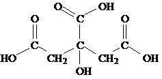
The peroxide based oxidative etches for GaAs are divided into acidic and basic etches. The composition and application of some of these systems are summarized in [link] . The most widely used of these is H 2 SO 4 /H 2 O 2 /H 2 O and is referred to as Caro's acid. The high viscosity of H 2 SO 4 results in diffusion-limited etching with high acid concentrations. Etches with low acid concentrations tend to be anisotropic. Phosphoric acid (H 3 PO 4 ) or citric acid ( [link] ) may be exchanged for sulfuric acid (H 2 SO 4 ). Replacement of the acid component with bases such as NH 4 OH or NaOH can result in near to truly isotropic etchants, although certain combinations can result in strong anisotropy.
| Formulation | Volume ratio | (100) etch rate (μm/min) | (110) etch rate (μm/min) | (111)As etch rate (μm/min) | (111)Ga etch rate (μm/min) |
| H 2 SO 4 / H 2 O 2 / H 2 O | 8:1:1 | 1.5 | 1.5 | 1.5 | 0.8 |
| H 2 SO 4 / H 2 O 2 / H 2 O | 1:8:1 | 8.0 | 8.0 | 12.0 | 3.0 |
| H 2 SO 4 / H 2 O 2 / H 2 O | 3:1:50 | 0.8 | 0.8 | 0.8 | 0.4 |
| citric acid/ H 2 O 2 / H 2 O | 1:1:1 | 0.6 | 0.6 | 0.6 | 0.4 |
| NH 4 OH/ H 2 O 2 / H 2 O | 1:700 | 0.3 | 0.3 | 0.3 | 0.3 |
| NaOH/ H 2 O 2 / H 2 O | 1:0.76 | 0.2 | 0.2 | 0.2 | 0.2 |
One of the earliest etching systems for GaAs is based on the use of a dilute (ca. 0.05 vol.%) solution of bromine (Br 2 ) in ethanol. The Br 2 acts as the oxidant, resulting in the formation of soluble bromides. The etch rate of this system is different for different crystallographic planes, i.e., the etch rates for the (111) As, (100), and (111) Ga faces are in the ratio 6:5:1, although more uniform etch rates are observed with high Br 2 concentrations (ca. 10 vol.%). These higher concentration solutions are used for the removal of damage due to cutting with the saw.
The purpose of polishing is to produce a smooth, specular surface on which device features can be defined by lithography. In order to allow for very large scale integration (VLSI) or ultra large scale integration (ULSI) fabrication the wafer must have a surface with a high degree of flatness. Variations less than 5 to 10 μm across the wafer diameter are typical flatness specifications. In addition, given the preceding steps, wafer polishing must not leave residual contamination or surface damage. The techniques of wafer polishing are derived from the glass lens industry, with some important modifications that have been developed to meet the special requirements of the microelectronics industry.
If the surface of a wafer that has undergone lapping (or grinding) is examined with an electron microscope, cracks, ridges and valleys are observed. The top "relief layer" consists of peaks and valleys. Below this layer is a damaged layer characterized by microcracks, dislocations, slip and stress. [link] shows a schematic representation of the abraded surface. Both of these layers must be removed completely prior to further fabrication. Decreasing the particle size of the abrasive during lapping only decreases the scale of the damage, but does not eliminate it entirely. In fact this surface damage is a characteristic of the brittle fracture of single crystal Si and GaAs, and occurs because during lapping the abrasive grains are moved across the surface under a pressure beyond that of the fracture strength of the wafer materials (Si or GaAs). In contrast to the mechanical abrasion employed in lapping, polishing is a mechano-chemical process during which brittle fracture does not occur. A polished wafer does not display any evidence of a relief surface such as that produced by lapping, even at highest resolution electron microscope.
Notification Switch
Would you like to follow the 'Chemistry of electronic materials' conversation and receive update notifications?

|
|

|
|

|
|

|
|

|
|
|
|

|
|
|
|
|

|
|
|
|