

| << Chapter < Page | Chapter >> Page > |

As stated earlier, it is a good approximation in thin film analysis that the total energy loss ΔE is proportional to depth t. With this approximation, we can derive the relation between energy width ΔE of the signal from a film of thickness Δt as follows,
ΔE = Δt( k dE/dx in + 1/cosØ dE/dx out )
where Ø = lab scattering angle.
It is worth noting that k is the kinematic factor defined in equation above and the subscripts “in” and “out” indicate the energies at which the rate of loss of energy or dE/dx is evaluated. As an example, we consider the backscattering spectrum, at scattering angle 170°, for 2 MeV He ++ incidents on silicon layer deposited onto 2 mm thick niobium substrate [link] .
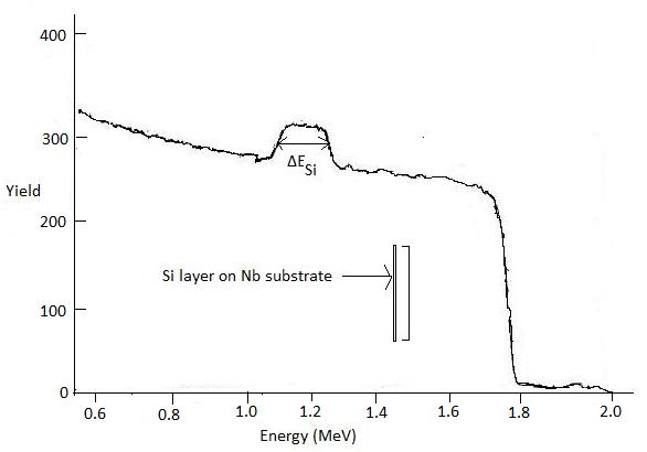
The energy loss rate of incoming He ++ or dE/dx along inward path in elemental Si is ≈24.6 eV/Å at 2 MeV and is ≈26 eV/Å for the outgoing particle at 1.12 MeV (Since K of Si is 0.56 when the scattering angle is 170°, energy of the outgoing particle would be equal to 2 x 0.56 or 1.12 MeV) . Again the value of ΔE Si is ≈133.3 keV. Putting the values into above equation we get
Δt ≈ 133.3 keV/(0.56 * 24.6 eV/Å + 1/cos 170° * 26 eV/Å)
= 133.3 keV/(13.77 eV/Å + 29/.985 eV/Å)
= 133.3 keV/ 40.17 eV/Å
= 3318 Å.
Hence a Si layer of ca. 3300 Å thickness has been deposited on the niobium substrate. However we need to remember that the value of dE/dx is approximated in this calculation.
In addition to depth profile analysis, we can study the composition of an element quantitatively by backscattering spectroscopy. The basic equation for quantitative analysis is
Y = σ. Ω. Q. NΔt
Where Y is the yield of scattered ions from a thin layer of thickness Δt, Q is the number of incident ions and Ω is the detector solid angle, and NΔt is the number of specimen atoms (atom/cm 2 ). [link] shows the RBS spectrum for a sample of silicon deposited on a niobium substrate and subjected to laser mixing. The Nb has reacted with the silicon to form a NbSi 2 interphase layer. The Nb signal has broadened after the reaction as show in [link] .

We can use ratio of the heights H Si /H Nb of the backscattering spectrum after formation of NbSi 2 to determine the composition of the silicide layer. The stoichiometric ratio of Nb and Si can be approximated as,
N Si /N Nb ≈ [H Si * σ Si ]/[H Nb * σ Nb ]
Hence the concentration of Si and Nb can be determined if we can know the appropriate cross sections σ Si and σ Nb . However the yield in the backscattering spectra is better represented as the product of signal height and the energy width ΔE. Thus stoichiometric ratio can be better approximated as
N Si /N Nb ≈ [H Si * ΔE Si * σ Si ]/[H Nb * ΔE Nb * σ Nb ]
It is of interest to understand the limitations of the backscattering technique in terms of the comparison with other thin film analysis technique such as AES, XPS and SIMS ( [link] ). AES has better mass resolution, lateral resolution and depth resolution than RBS. But AES suffers from sputtering artifacts. Compared to RBS, SIMS has better sensitivity. RBS does not provide any chemical bonding information which we can get from XPS. Again, sputtering artifact problems are also associated in XPS. The strength of RBS lies in quantitative analysis. However, conventional RBS systems cannot analyze ultrathin films since the depth resolution is only about 10 nm using surface barrier detector.
Rutherford Backscattering analysis is a straightforward technique to determine the thickness and composition of thin films (<4000 Å). Areas that have been lately explored are the use of backscattering technique in composition determination of new superconductor oxides; analysis of lattice mismatched epitaxial layers, and as a probe of thin film morphology and surface clustering.
Notification Switch
Would you like to follow the 'Physical methods in chemistry and nano science' conversation and receive update notifications?

|
|

|
|

|
|

|
|

|
|

|
|

|
|

|
|

|
|

|