<< Chapter < Page Chapter >> Page >

Vacancies

The converse of an interstitial impurity is when there are not enough atoms in a particular area of the lattice. These are called vacancies. Vacancies exist in any material above absolute zero and increase in concentration with temperature. In the case of compound semiconductors, vacancies can be either cation vacancies ( [link] c) or anion vacancies ( [link] d), depending on what type of atom are “missing”.

Substitution

Substitution of various atoms into the normal lattice structure is common, and used to change the electronic properties of both compound and elemental semiconductors. Any impurity element that is incorporated during crystal growth can occupy a lattice site. Depending on the impurity, substitution defects can greatly distort the lattice and/or alter the electronic structure. In general, cations will try to occupy cation lattice sites ( [link] e), and anion will occupy the anion site ( [link] f). For example, a zinc impurity in GaAs will occupy a gallium site, if possible, while a sulfur, selenium and tellurium atoms would all try to substitute for an arsenic. Some impurities will occupy either site indiscriminately, e.g., Si and Sn occupy both Ga and As sites in GaAs.

Antisite defects

Antisite defects are a particular form of substitution defect, and are unique to compound semiconductors. An antisite defect occurs when a cation is misplaced on an anion lattice site or vice versa ( [link] g and h). Dependant on the arrangement these are designated as either A B antisite defects or B A antisite defects. For example, if an arsenic atom is on a gallium lattice site the defect would be an As Ga defect. Antisite defects involve fitting into a lattice site atoms of a different size than the rest of the lattice, and therefore this often results in a localized distortion of the lattice. In addition, cations and anions will have a different number of electrons in their valence shells, so this substitution will alter the local electron concentration and the electronic properties of this area of the semiconductor.

Extended defects: dislocations in a crystal lattice

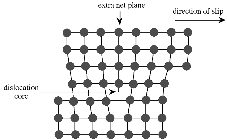
Extended defects may be created either during crystal growth or as a consequence of stress in the crystal lattice. The plastic deformation of crystalline solids does not occur such that all bonds along a plane are broken and reformed simultaneously. Instead, the deformation occurs through a dislocation in the crystal lattice. [link] shows a schematic representation of a dislocation in a crystal lattice. Two features of this type of dislocation are the presence of an extra crystal plane, and a large void at the dislocation core. Impurities tend to segregate to the dislocation core in order to relieve strain from their presence.

Dislocation in a crystal lattice.

Epitaxy

Epitaxy, is a transliteration of two Greek words epi , meaning "upon", and taxis , meaning "ordered". With respect to crystal growth it applies to the process of growing thin crystalline layers on a crystal substrate. In epitaxial growth, there is a precise crystal orientation of the film in relation to the substrate. The growth of epitaxial films can be done by a number of methods including molecular beam epitaxy, atomic layer epitaxy, and chemical vapor deposition, all of which will be described later.

Epitaxy of the same material, such as a gallium arsenide film on a gallium arsenide substrate, is called homoepitaxy, while epitaxy where the film and substrate material are different is called heteroepitaxy. Clearly, in homoepitaxy, the substrate and film will have the identical structure, however, in heteroepitaxy, it is important to employ where possible a substrate with the same structure and similar lattice parameters. For example, zinc selenide (zinc blende, a = 5.668 Å) is readily grown on gallium arsenide (zinc blende, a = 5.653 Å). Alternatively, epitaxial crystal growth can occur where there exists a simple relationship between the structures of the substrate and crystal layer, such as is observed between Al 2 O 3 (100) on Si (100). Whichever route is chosen a close match in the lattice parameters is required, otherwise, the strains induced by the lattice mismatch results in distortion of the film and formation of dislocations. If the mismatch is significant epitaxial growth is not energetically favorable, causing a textured film or polycrystalline untextured film to be grown. As a general rule of thumb, epitaxy can be achieved if the lattice parameters of the two materials are within about 5% of each other. For good quality epitaxy, this should be less than 1%. The larger the mismatch, the larger the strain in the film. As the film gets thicker and thicker, it will try to relieve the strain in the film, which could include the loss of epitaxy of the growth of dislocations. It is important to note that the<100>directions of a film must be parallel to the<100>direction of the substrate. In some cases, such as Fe on MgO, the [111] direction is parallel to the substrate [100]. The epitaxial relationship is specified by giving first the plane in the film that is parallel to the substrate [100].

Bibliography

  • International Tables for X-ray Crystallography . Vol. IV; Kynoch Press: Birmingham, UK (1974).
  • B. F. G. Johnson, in Comprehensive Inorganic Chemistry , Pergamon Press, Vol. 4, Chapter 52 (1973).
  • A. R. West, Solid State Chemistry and its Applications , Wiley, New York (1984).

Questions & Answers

differentiate between demand and supply giving examples
Lambiv Reply
differentiated between demand and supply using examples
Lambiv
what is labour ?
Lambiv
how will I do?
Venny Reply
how is the graph works?I don't fully understand
Rezat Reply
information
Eliyee
devaluation
Eliyee
t
WARKISA
hi guys good evening to all
Lambiv
multiple choice question
Aster Reply
appreciation
Eliyee
explain perfect market
Lindiwe Reply
In economics, a perfect market refers to a theoretical construct where all participants have perfect information, goods are homogenous, there are no barriers to entry or exit, and prices are determined solely by supply and demand. It's an idealized model used for analysis,
Ezea
What is ceteris paribus?
Shukri Reply
other things being equal
AI-Robot
When MP₁ becomes negative, TP start to decline. Extuples Suppose that the short-run production function of certain cut-flower firm is given by: Q=4KL-0.6K2 - 0.112 • Where is quantity of cut flower produced, I is labour input and K is fixed capital input (K-5). Determine the average product of lab
Kelo
Extuples Suppose that the short-run production function of certain cut-flower firm is given by: Q=4KL-0.6K2 - 0.112 • Where is quantity of cut flower produced, I is labour input and K is fixed capital input (K-5). Determine the average product of labour (APL) and marginal product of labour (MPL)
Kelo
yes,thank you
Shukri
Can I ask you other question?
Shukri
what is monopoly mean?
Habtamu Reply
What is different between quantity demand and demand?
Shukri Reply
Quantity demanded refers to the specific amount of a good or service that consumers are willing and able to purchase at a give price and within a specific time period. Demand, on the other hand, is a broader concept that encompasses the entire relationship between price and quantity demanded
Ezea
ok
Shukri
how do you save a country economic situation when it's falling apart
Lilia Reply
what is the difference between economic growth and development
Fiker Reply
Economic growth as an increase in the production and consumption of goods and services within an economy.but Economic development as a broader concept that encompasses not only economic growth but also social & human well being.
Shukri
production function means
Jabir
What do you think is more important to focus on when considering inequality ?
Abdisa Reply
any question about economics?
Awais Reply
sir...I just want to ask one question... Define the term contract curve? if you are free please help me to find this answer 🙏
Asui
it is a curve that we get after connecting the pareto optimal combinations of two consumers after their mutually beneficial trade offs
Awais
thank you so much 👍 sir
Asui
In economics, the contract curve refers to the set of points in an Edgeworth box diagram where both parties involved in a trade cannot be made better off without making one of them worse off. It represents the Pareto efficient allocations of goods between two individuals or entities, where neither p
Cornelius
In economics, the contract curve refers to the set of points in an Edgeworth box diagram where both parties involved in a trade cannot be made better off without making one of them worse off. It represents the Pareto efficient allocations of goods between two individuals or entities,
Cornelius
Suppose a consumer consuming two commodities X and Y has The following utility function u=X0.4 Y0.6. If the price of the X and Y are 2 and 3 respectively and income Constraint is birr 50. A,Calculate quantities of x and y which maximize utility. B,Calculate value of Lagrange multiplier. C,Calculate quantities of X and Y consumed with a given price. D,alculate optimum level of output .
Feyisa Reply
Answer
Feyisa
c
Jabir
the market for lemon has 10 potential consumers, each having an individual demand curve p=101-10Qi, where p is price in dollar's per cup and Qi is the number of cups demanded per week by the i th consumer.Find the market demand curve using algebra. Draw an individual demand curve and the market dema
Gsbwnw Reply
suppose the production function is given by ( L, K)=L¼K¾.assuming capital is fixed find APL and MPL. consider the following short run production function:Q=6L²-0.4L³ a) find the value of L that maximizes output b)find the value of L that maximizes marginal product
Abdureman
types of unemployment
Yomi Reply
What is the difference between perfect competition and monopolistic competition?
Mohammed
Got questions? Join the online conversation and get instant answers!
Jobilize.com Reply

Get Jobilize Job Search Mobile App in your pocket Now!

Get it on Google Play Download on the App Store Now


Source:  OpenStax, Physical methods in chemistry and nano science. OpenStax CNX. May 05, 2015 Download for free at http://legacy.cnx.org/content/col10699/1.21
Google Play and the Google Play logo are trademarks of Google Inc.

Notification Switch

Would you like to follow the 'Physical methods in chemistry and nano science' conversation and receive update notifications?

Ask