

| << Chapter < Page | Chapter >> Page > |
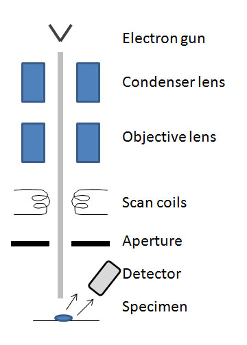
The SEM is made of several main components: electron gun, condenser lens, scan coils, detectors, specimen, and lenses (see [link] ). Today, portable SEMs are available but the typical size is about 6 feet tall and contains the microscope column and the control console.
A special feature of the SEM and TEM is known as depth of focus , dv/du the range of positions (depths) at which the image can be viewed with good focus, see [link] . This allows the user to see more than a singular plane of a specified height in focus and essentially allows a range of three dimensional imaging.
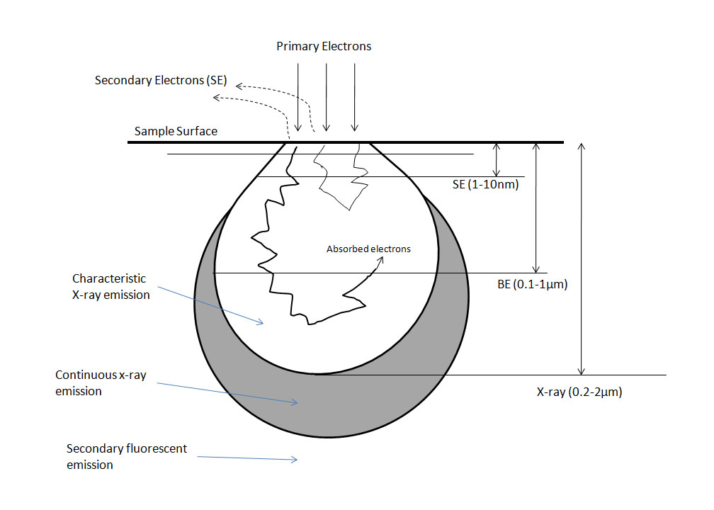
The secondary electron detector (SED) is the main source of SEM images since a large majority of the electrons emitted from the sample are less than 50 eV. These electrons form textural images but cannot determine composition. The SEM may also be equipped with a backscatter electron detector (BSED) which collects the higher energy BSE’s. Backscattered electrons are very sensitive to atomic number and can determine qualitative information about nuclei present (i.e., how much Fe is in the sample). Topographic images are taken by tilting the specimen 20 - 40° toward the detector. With the sample tilted, electrons are more likely to scatter off the top of the sample rather than interact within it, thus yielding information about the surface.
The most effective SEM sample will be at least as thick as the interaction volume; depending on the image technique you are using (typically at least 2 µm). For the best contrast, the sample must be conductive or the sample can be sputter-coated with a metal (such as Au, Pt, W, and Ti). Metals and other materials that are naturally conductive do not need to be coated and need very little sample preparation.
As previously discussed, to view features that are smaller than the wavelength of light, an electron microscope must be used. The electron beam requires extremely high vacuum to protect the filament and electrons must be able to adequately interact with the sample. Polymers are typically long chains of repeating units composed primarily of “lighter” (low atomic number) elements such as carbon, hydrogen, nitrogen, and oxygen. These lighter elements have fewer interactions with the electron beam which yields poor contrast, so often times a stain or coating is required to view polymer samples. SEM imaging requires a conductive surface, so a large majority of polymer samples are sputter coated with metals, such as gold.
The decision to view a polymer sample with an SEM (versus a TEM for example) should be evaluated based on the feature size you expect the sample to have. Generally, if you expect the polymer sample to have features, or even individual molecules, over 100 nm in size you can safely choose SEM to view your sample. For much smaller features, the TEM may yield better results, but requires much different sample preparation than will be described here.
Notification Switch
Would you like to follow the 'Physical methods in chemistry and nano science' conversation and receive update notifications?

|
|

|
|

|
|

|
|

|
|

|
|

|
|

|
|

|
|

|