

| << Chapter < Page | Chapter >> Page > |

One improvement that can be made to the above system is to replace the floodlight with a simple slide projector. The floodlight will typically have a spectrum very heavily weighted in the red and infrared and will be deficient in the shorter wavelengths. Though still not a perfect match to the solar spectrum, the slide projector does at least have more output at the shorter wavelengths; at the same time it will have less IR output compared to the floodlight and the combination should give a somewhat more representative response. A typical set up is shown in [link] .

The mirror in [link] serves two purposes. First, it turns the beam so the test object can be laid flat a measurement bed and second it serves to collimate and concentrate the beam by focusing it on a smaller area, giving a better approximation of terrestrial solar intensity over a range of intensities such as AM2 (air mass 2) through AM0 ( [link] ). An estimate of the intensity can be made using a calibrated silicon solar cell of the sort that can be purchased online from any of several scientific hobby shops such as Edmunds Scientific. While still far from enabling a quantitative measurement of device output, the technique will at least provide indications within a ballpark range of actual cell efficiency.

[link] shows a measurement made with the test device placed at a distance from the mirror for which the intensity was previously determined to be equivalent to AM1 solar intensity, or 1000 watts per square meter. Since the beam passes through the projector lens and reflects from the second surface of the slightly concave mirror, there is essentially no UV light left in the beam that could be harmful to the naked eye. Still, if this technique is used, it is recommended that observations be made through a piece of ordinary glass such as eyeglasses or even a small glass shield inserted for that purpose. The blue area in the figure represents the largest rectangle that can be drawn under the curve and gives the maximum output power of the cell, which is simply the product of the current and voltage at maximum power.
If the power density of the incident light (P 0 ) is known in W/cm 2 , the device efficiency can be obtained by dividing the maximum power (as determined from I m and V m ) by the incident power density times the area of the cell (A cell ), [link] .

In many cases it is beneficial to determine the photoconductivity of a new material prior to cell fabrication. This allows for the rapid screening of materials or synthesis variable of a single material even before issues of cell design and construction are considered.
[link] shows the circuit diagram of a simple photoconductivity test made with a slightly different set up compared to that shown above. In this case a voltage is placed across the sample after it has been connected to a resistor placed in series with the sample. A simple 9 V battery secured with a battery holder or a small ac to dc power converter can be used to supply the voltage. The sample and resistor sit inside a small box with an open top.
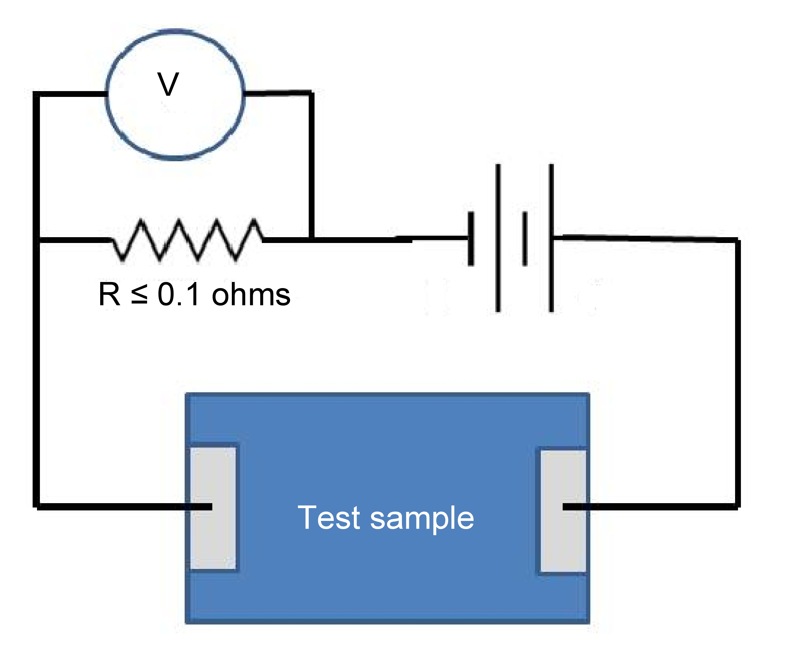
The voltage across (in this case) the 10 ohm resister was measured with a shutter held over the sample (a simple piece of cardboard sitting on the top of the box) and with the shutter removed. The difference in voltage is a direct indication of the change in the photoconductance of the sample and again is a very quick and simple test to see if the material being developed does indeed have a photoresponse of some sort without having to make a full device structure. Adjusting the position of the light source so that the incident light power density at the sample surface is 200 or 500 or 1000 W/m 2 enables an approximate numerical estimate of the photocurrent that was generated and again can help guide the development of new materials for solar cell applications. The results from such a measurement are shown in [link] for a sample of carbon nanotubes (CNT) coated with CdSe by liquid phase deposition (LPD).

Notification Switch
Would you like to follow the 'Physical methods in chemistry and nano science' conversation and receive update notifications?

|
|

|
|

|
|

|
|

|
|

|
|

|
|

|
|
|
|
|

|