

| << Chapter < Page | Chapter >> Page > |
Low energy electron diffraction (LEED) is a very powerful technique that allows for the characterization of the surface of materials. Its high surface sensitivity is due to the use of electrons with energies between 20-200 eV, which have wavelengths equal to 2.7 – 0.87 Å (comparable to the atomic spacing). Therefore, the electrons can be elastically scattered easily by the atoms in the first few layers of the sample. Its features, such as little penetration of low–energy electrons have positioned it as one of the most common techniques in surface science for the determination of the symmetry of the unit cell (qualitative analysis) and the position of the atoms in the crystal surface (quantitative analysis).
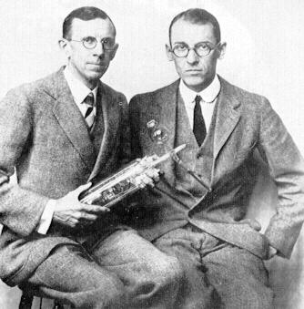
In 1924 Louis de Brogile postulated that all forms of matter, such as electrons, have a wave-particle nature. Three years later after this postulate, the American physicists Clinton J. Davisson and Lester H. Germer ( [link] ) proved experimentally the wave nature of electrons at Bell Labs in New York, see Figure 1. At that time, they were investigating the distribution-in-angle of the elastically scattered electrons (electrons that have suffered no loss of kinetic energy) from the (111) face of a polycrystalline nickel, material composed of many randomly oriented crystals.
The experiment consisted of a beam of electrons from a heated tungsten filament directed against the polycrystalline nickel and an electron detector, which was mounted on an arc to observe the electrons at different angles. During the experiment, air entered in the vacuum chamber where the nickel was, producing an oxide layer on its surface. Davisson and Clinton reduced the nickel by heating it at high temperature. They did not realize that the thermal treatment changed the polycrystalline nickel to a nearly monocrystalline nickel, material composed of many oriented crystals. When they repeated the experiment, it was a great surprise that the distribution-in-angle of the scattered electrons manifested sharp peaks at certain angles. They soon realized that these peaks were interference patterns, and, in analogy to X-ray diffraction, the arrangement of atoms and not the structure of the atoms was responsible for the pattern of the scattered electrons.
The results of Davisson and Germer were soon corroborated by George Paget Thomson, J. J. Thomson’s son. In 1937, both Davisson and Thomson were awarded with the Nobel Prize in Physics for their experimental discovery of the electron diffraction by crystals. It is noteworthy that 31 years after J. J. Thomson showed that the electron is a particle, his son showed that it is also a wave.
Although the discovery of low-energy electron diffraction was in 1927, it became popular in the early 1960’s, when the advances in electronics and ultra-high vacuum technology made possible the commercial availability of LEED instruments. At the beginning, this technique was only used for qualitative characterization of surface ordering. Years later, the impact of computational technologies allowed the use of LEED for quantitative analysis of the position of atoms within a surface. This information is hidden in the energetic dependence of the diffraction spot intensities, which can be used to construct a LEED I-V curve.
Notification Switch
Would you like to follow the 'Physical methods in chemistry and nano science' conversation and receive update notifications?

|
|

|
|

|
|

|
|

|
|

|
|

|
|

|
|

|
|

|