<< Chapter < Page Chapter >> Page >
By the end of this section, you will be able to:
  • Describe what occurs when n- and p-type materials are joined together using the concept of diffusion and drift current (zero applied voltage)
  • Explain the response of a p-n junction to a forward and reverse bias voltage
  • Describe the function of a transistor in an electric circuit
  • Use the concept of a p-n junction to explain its applications in audio amplifiers and computers

Semiconductors have many applications in modern electronics. We describe some basic semiconductor devices in this section. A great advantage of using semiconductors for circuit elements is the fact that many thousands or millions of semiconductor devices can be combined on the same tiny piece of silicon and connected by conducting paths. The resulting structure is called an integrated circuit (ic), and ic chips are the basis of many modern devices, from computers and smartphones to the internet and global communications networks.

Diodes

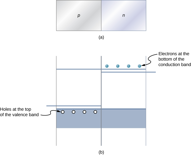
Perhaps the simplest device that can be created with a semiconductor is a diode. A diode is a circuit element that allows electric current to flow in only one direction, like a one-way valve (see Model of Conduction in Metals ). A diode is created by joining a p -type semiconductor to an n -type semiconductor ( [link] ). The junction between these materials is called a p-n junction    . A comparison of the energy bands of a silicon-based diode is shown in [link] (b). The positions of the valence and conduction bands are the same, but the impurity levels are quite different. When a p-n junction is formed, electrons from the conduction band of the n -type material diffuse to the p -side, where they combine with holes in the valence band. This migration of charge leaves positive ionized donor ions on the n -side and negative ionized acceptor ions on the p -side, producing a narrow double layer of charge at the p - n junction called the depletion layer    . The electric field associated with the depletion layer prevents further diffusion. The potential energy for electrons across the p-n junction is given by [link] .

Figure a shows two blocks place side by side, in contact. The left one is labeled p and the right one is labeled n. Figure b shows a valence band at the bottom and a conduction band at the top. There are holes within the valance band on the left, labeled holes at the top of the valence band. There are electrons above the conduction line on the right, labeled electrons at the bottom of the conduction band. Impurity bands are shown above the holes and below the electrons.
(a) Representation of a p-n junction. (b) A comparison of the energy bands of p -type and n -type silicon prior to equilibrium.
Figure a shows two blocks place side by side, in contact. The left one is labeled p and the right one is labeled n. Minus signs are shown in the p block near the side in contact. Plus signs are shown in the n block near the side in contact. Figure b shows a valence band at the bottom and a conduction line at the top. The valence band is higher on the left side almost reaching the central line between the two bands. There are holes with the valence band at the top, on the left. The conduction line is lower on the right, almost reaching the central line between the two bands. There are electrons just above the line, on the right. The displacement of the bands is labeled eV subscript 0, potential difference prevents diffusion of electrons from n side to p side.
At equilibrium, (a) excess charge resides near the interface and the net current is zero, and (b) the potential energy difference for electrons (in light blue) prevents further diffusion of electrons into the p -side.

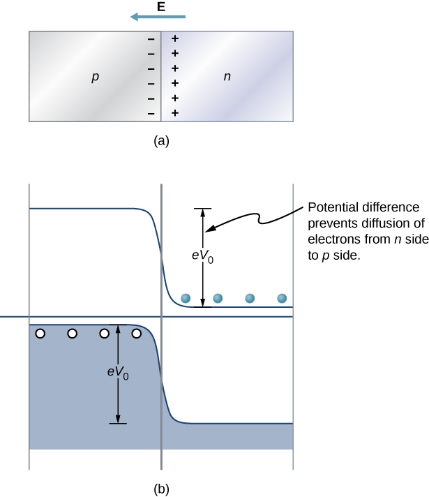
The behavior of a semiconductor diode can now be understood. If the positive side of the battery is connected to the n -type material, the depletion layer is widened, and the potential energy difference across the p-n junction is increased. Few or none of the electrons (holes) have enough energy to climb the potential barrier, and current is significantly reduced. This is called the reverse bias configuration    . On the other hand, if the positive side of a battery is connected to the p -type material, the depletion layer is narrowed, the potential energy difference across the p-n junction is reduced, and electrons (holes) flow easily. This is called the forward bias configuration    of the diode. In sum, the diode allows current to flow freely in one direction but prevents current flow in the opposite direction. In this sense, the semiconductor diode is a one-way valve.

Questions & Answers

how does Neisseria cause meningitis
Nyibol Reply
what is microbiologist
Muhammad Reply
what is errata
Muhammad
is the branch of biology that deals with the study of microorganisms.
Ntefuni Reply
What is microbiology
Mercy Reply
studies of microbes
Louisiaste
when we takee the specimen which lumbar,spin,
Ziyad Reply
How bacteria create energy to survive?
Muhamad Reply
Bacteria doesn't produce energy they are dependent upon their substrate in case of lack of nutrients they are able to make spores which helps them to sustain in harsh environments
_Adnan
But not all bacteria make spores, l mean Eukaryotic cells have Mitochondria which acts as powerhouse for them, since bacteria don't have it, what is the substitution for it?
Muhamad
they make spores
Louisiaste
what is sporadic nd endemic, epidemic
Aminu Reply
the significance of food webs for disease transmission
Abreham
food webs brings about an infection as an individual depends on number of diseased foods or carriers dully.
Mark
explain assimilatory nitrate reduction
Esinniobiwa Reply
Assimilatory nitrate reduction is a process that occurs in some microorganisms, such as bacteria and archaea, in which nitrate (NO3-) is reduced to nitrite (NO2-), and then further reduced to ammonia (NH3).
Elkana
This process is called assimilatory nitrate reduction because the nitrogen that is produced is incorporated in the cells of microorganisms where it can be used in the synthesis of amino acids and other nitrogen products
Elkana
Examples of thermophilic organisms
Shu Reply
Give Examples of thermophilic organisms
Shu
advantages of normal Flora to the host
Micheal Reply
Prevent foreign microbes to the host
Abubakar
they provide healthier benefits to their hosts
ayesha
They are friends to host only when Host immune system is strong and become enemies when the host immune system is weakened . very bad relationship!
Mark
what is cell
faisal Reply
cell is the smallest unit of life
Fauziya
cell is the smallest unit of life
Akanni
ok
Innocent
cell is the structural and functional unit of life
Hasan
is the fundamental units of Life
Musa
what are emergency diseases
Micheal Reply
There are nothing like emergency disease but there are some common medical emergency which can occur simultaneously like Bleeding,heart attack,Breathing difficulties,severe pain heart stock.Hope you will get my point .Have a nice day ❣️
_Adnan
define infection ,prevention and control
Innocent
I think infection prevention and control is the avoidance of all things we do that gives out break of infections and promotion of health practices that promote life
Lubega
Heyy Lubega hussein where are u from?
_Adnan
en français
Adama
which site have a normal flora
ESTHER Reply
Many sites of the body have it Skin Nasal cavity Oral cavity Gastro intestinal tract
Safaa
skin
Asiina
skin,Oral,Nasal,GIt
Sadik
How can Commensal can Bacteria change into pathogen?
Sadik
How can Commensal Bacteria change into pathogen?
Sadik
all
Tesfaye
by fussion
Asiina
what are the advantages of normal Flora to the host
Micheal
what are the ways of control and prevention of nosocomial infection in the hospital
Micheal
what is inflammation
Shelly Reply
part of a tissue or an organ being wounded or bruised.
Wilfred
what term is used to name and classify microorganisms?
Micheal Reply
Binomial nomenclature
adeolu
Got questions? Join the online conversation and get instant answers!
Jobilize.com Reply
Practice Key Terms 9

Get Jobilize Job Search Mobile App in your pocket Now!

Get it on Google Play Download on the App Store Now


Source:  OpenStax, University physics volume 3. OpenStax CNX. Nov 04, 2016 Download for free at http://cnx.org/content/col12067/1.4
Google Play and the Google Play logo are trademarks of Google Inc.

Notification Switch

Would you like to follow the 'University physics volume 3' conversation and receive update notifications?

Ask