<< Chapter < Page Chapter >> Page >
By the end of this section, you will be able to:
  • Describe changes to the energy structure of a semiconductor due to doping
  • Distinguish between an n-type and p-type semiconductor
  • Describe the Hall effect and explain its significance
  • Calculate the charge, drift velocity, and charge carrier number density of a semiconductor using information from a Hall effect experiment

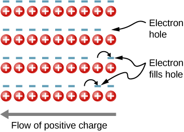
In the preceding section, we considered only the contribution to the electric current due to electrons occupying states in the conduction band. However, moving an electron from the valence band to the conduction band leaves an unoccupied state or hole    in the energy structure of the valence band, which a nearby electron can move into. As these holes are filled by other electrons, new holes are created. The electric current associated with this filling can be viewed as the collective motion of many negatively charged electrons or the motion of the positively charged electron holes.

To illustrate, consider the one-dimensional lattice in [link] . Assume that each lattice atom contributes one valence electron to the current. As the hole on the right is filled, this hole moves to the left. The current can be interpreted as the flow of positive charge to the left. The density of holes, or the number of holes per unit volume, is represented by p . Each electron that transitions into the conduction band leaves behind a hole. If the conduction band is originally empty, the conduction electron density p is equal to the hole density, that is, n = p .

Figure shows four pairs of rows. Each pair has a top row of minus signs and a bottom row of circles with plus signs in them. An arrow labeled flow of positive charge points left. In the second row of minus signs, the last minus sign is missing. The empty space is labeled electron hole. In the third row of minus signs, the second to last minus sign is missing. An arrow is shown from here to the last minus sign. This is labeled electron fills hole. Similarly, in the fourth row of minus signs, the third from last minus sign is missing. An arrow is shown from here to the second to last minus sign. This is also labeled electron fills hole.
The motion of holes in a crystal lattice. As electrons shift to the right, an electron hole moves to the left.

As mentioned, a semiconductor is a material with a filled valence band, an unfilled conduction band, and a relatively small energy gap between the bands. Excess electrons or holes can be introduced into the material by the substitution into the crystal lattice of an impurity atom    , which is an atom of a slightly different valence number. This process is known as doping    . For example, suppose we add an arsenic atom to a crystal of silicon ( [link] (a)).

Figure a shows a grid with circles marked silicon atoms on each junction. On one junction, is a different colored circle labeled arsenic atom. A small circle is shown in between the silicon atoms. This is labeled extra electron from arsenic atom. Figure b shows a grid with circles marked silicon atoms on each junction. On one junction, is a different colored circle labeled aluminum atom. A small circle is shown in between the silicon atoms. This is labeled hole.
(a) A donor impurity and (b) an acceptor impurity. The introduction to impurities and acceptors into a semiconductor significantly changes the electronic properties of this material.

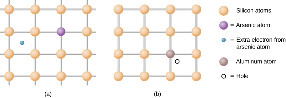
Arsenic has five valence electrons, whereas silicon has only four. This extra electron must therefore go into the conduction band, since there is no room in the valence band. The arsenic ion left behind has a net positive charge that weakly binds the delocalized electron. The binding is weak because the surrounding atomic lattice shields the ion’s electric field. As a result, the binding energy of the extra electron is only about 0.02 eV. In other words, the energy level of the impurity electron is in the band gap below the conduction band by 0.02 eV, a much smaller value than the energy of the gap, 1.14 eV. At room temperature, this impurity electron is easily excited into the conduction band and therefore contributes to the conductivity ( [link] (a)). An impurity with an extra electron is known as a donor impurity    , and the doped semiconductor is called an n -type semiconductor    because the primary carriers of charge (electrons) are negative.

Questions & Answers

what is biology
Hajah Reply
the study of living organisms and their interactions with one another and their environments
AI-Robot
what is biology
Victoria Reply
HOW CAN MAN ORGAN FUNCTION
Alfred Reply
the diagram of the digestive system
Assiatu Reply
allimentary cannel
Ogenrwot
How does twins formed
William Reply
They formed in two ways first when one sperm and one egg are splited by mitosis or two sperm and two eggs join together
Oluwatobi
what is genetics
Josephine Reply
Genetics is the study of heredity
Misack
how does twins formed?
Misack
What is manual
Hassan Reply
discuss biological phenomenon and provide pieces of evidence to show that it was responsible for the formation of eukaryotic organelles
Joseph Reply
what is biology
Yousuf Reply
the study of living organisms and their interactions with one another and their environment.
Wine
discuss the biological phenomenon and provide pieces of evidence to show that it was responsible for the formation of eukaryotic organelles in an essay form
Joseph Reply
what is the blood cells
Shaker Reply
list any five characteristics of the blood cells
Shaker
lack electricity and its more savely than electronic microscope because its naturally by using of light
Abdullahi Reply
advantage of electronic microscope is easily and clearly while disadvantage is dangerous because its electronic. advantage of light microscope is savely and naturally by sun while disadvantage is not easily,means its not sharp and not clear
Abdullahi
cell theory state that every organisms composed of one or more cell,cell is the basic unit of life
Abdullahi
is like gone fail us
DENG
cells is the basic structure and functions of all living things
Ramadan
What is classification
ISCONT Reply
is organisms that are similar into groups called tara
Yamosa
in what situation (s) would be the use of a scanning electron microscope be ideal and why?
Kenna Reply
A scanning electron microscope (SEM) is ideal for situations requiring high-resolution imaging of surfaces. It is commonly used in materials science, biology, and geology to examine the topography and composition of samples at a nanoscale level. SEM is particularly useful for studying fine details,
Hilary
cell is the building block of life.
Condoleezza Reply
Got questions? Join the online conversation and get instant answers!
Jobilize.com Reply

Get Jobilize Job Search Mobile App in your pocket Now!

Get it on Google Play Download on the App Store Now


Source:  OpenStax, University physics volume 3. OpenStax CNX. Nov 04, 2016 Download for free at http://cnx.org/content/col12067/1.4
Google Play and the Google Play logo are trademarks of Google Inc.

Notification Switch

Would you like to follow the 'University physics volume 3' conversation and receive update notifications?

Ask