| << Chapter < Page | Chapter >> Page > |
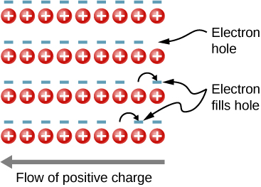
In the preceding section, we considered only the contribution to the electric current due to electrons occupying states in the conduction band. However, moving an electron from the valence band to the conduction band leaves an unoccupied state or hole in the energy structure of the valence band, which a nearby electron can move into. As these holes are filled by other electrons, new holes are created. The electric current associated with this filling can be viewed as the collective motion of many negatively charged electrons or the motion of the positively charged electron holes.
To illustrate, consider the one-dimensional lattice in [link] . Assume that each lattice atom contributes one valence electron to the current. As the hole on the right is filled, this hole moves to the left. The current can be interpreted as the flow of positive charge to the left. The density of holes, or the number of holes per unit volume, is represented by p . Each electron that transitions into the conduction band leaves behind a hole. If the conduction band is originally empty, the conduction electron density p is equal to the hole density, that is, .

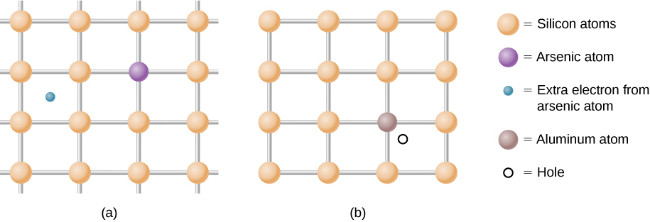
As mentioned, a semiconductor is a material with a filled valence band, an unfilled conduction band, and a relatively small energy gap between the bands. Excess electrons or holes can be introduced into the material by the substitution into the crystal lattice of an impurity atom , which is an atom of a slightly different valence number. This process is known as doping . For example, suppose we add an arsenic atom to a crystal of silicon ( [link] (a)).

Arsenic has five valence electrons, whereas silicon has only four. This extra electron must therefore go into the conduction band, since there is no room in the valence band. The arsenic ion left behind has a net positive charge that weakly binds the delocalized electron. The binding is weak because the surrounding atomic lattice shields the ion’s electric field. As a result, the binding energy of the extra electron is only about 0.02 eV. In other words, the energy level of the impurity electron is in the band gap below the conduction band by 0.02 eV, a much smaller value than the energy of the gap, 1.14 eV. At room temperature, this impurity electron is easily excited into the conduction band and therefore contributes to the conductivity ( [link] (a)). An impurity with an extra electron is known as a donor impurity , and the doped semiconductor is called an n -type semiconductor because the primary carriers of charge (electrons) are negative.

Notification Switch
Would you like to follow the 'University physics volume 3' conversation and receive update notifications?