

| << Chapter < Page | Chapter >> Page > |
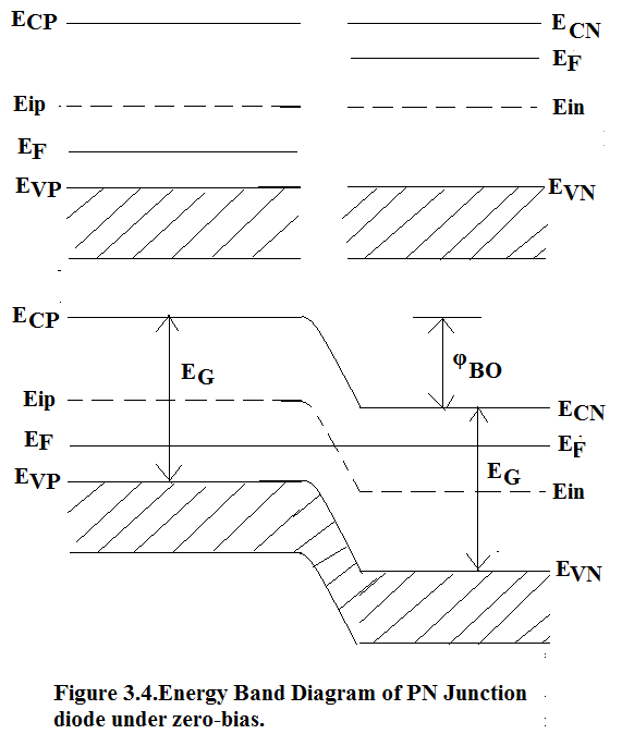
From Equation (3.2.12), it is evident that Built-in Barrier Potential is of the order of the Band-Gap of the material. Large Band-Gap material such as GaAs will have a large Built-in Barrier Potential and Narrow Band-Gap material such as Ge has a low Built-in Barrier Potential. This is the reason why Ge has a cut-in voltage of 0V, Si has 0.5V and Ga As has 1V.
Equation (3.2.12) also tells us that when doping approaches equivalent density of states, φ BO (Built-in Barrier Potential) approaches V G (Band-Gap Volt) and E F (Fermi-Level) enters the conduction band and valence band in N-Type and P-Type semiconductor respectively as shown in Figure (3.5). The semi-conductor becomes de-generate and Maxwell-Boltzmann Approzimation does not hold good and we must apply Fermi-Dirac Distribution.
Degenerate Semiconductor is referred to as semi-metal. Al(Aluminum) is P-Type material and when deposited over lightly doped N-Type material, PN junction is a rectifying contact and is referred to as Schottky Diode, hot electron diode.It has a very high switching speed.This technique is used in Scottky-clamped TTL gate,74 series. But if Al contact is deposited over N+ layer then we get ohmic contact. In vertical IC npn transistor, this technique is used for making contact to the Collector of the BJT.

3.2.2.PN Jn Diode under forward bias and theoretical deduction of Shockley Equation or Ideal Diode Equation..

Under forward bias, depletion layer shrinks,E max reduces and built-in barrier potential reduces by V F and majority carriers easily climb over the up-hill potential gradient and get injected to the other side strongly perturbing the minority carrier there-on.
If the forward bias is more than 0.5V which is the cut-in voltage for Si-Diode, PN Jn Diode turns on and there is exponential increase in the diffusion current whereas drift current remains unaltered. Drift current remains unaltered because it depends on the minority carriers falling down the potential gradient in the depletion width. Since minority carriers are in very short supply hence their drift is unaffected by forward bias.But the barrier potential which was of 0.8V drastically reduces for forward voltage greater than 0.5V hence majority carriers easily cross the up-hill potential gradient within the depletion and lead to a decade increase in the forward current for every 60mV increase in the forward bias which we will see in the next section.
Forward Current Density flow , its components and carrier concentration profiles under forward bias condition are shown in Figure 3.7.
As can be seen in Figure 3.7, majority carriers are injected to the oher side strongly perturbing the minority carrier from thermal equilibrium value to a new elevated value under forward bias condition. For example on N-Side:


These new perturbations p n (0) at the edge of the depletion layer on N-side and n p ( 0) at the edge of the depletion layer on P-side exponentially decay to thermal equilibrium values on their respective sides with length constant of L p and L n as shown in Figure 3.7.
Notification Switch
Would you like to follow the 'Solid state physics and devices-the harbinger of third wave of civilization' conversation and receive update notifications?

|
|

|
|

|
|

|
|

|
|

|
|

|
|

|
|

|
|

|