

| << Chapter < Page | Chapter >> Page > |
SSPD_Chapter 7_Part 3_Basic Electrical Properties_continued4.
7.3.11 Alternative forms of NAND Gates/Alternative forms of Pull-up configuration.
Just like RTL Logic, MOS Logic can have a passive load or an active load. From integration point of view we always prefer an active load in comparison to passive load.
Passive Load is a resistance and resistance occupies too much real estate on the chip as well as it has a limited options. Therefore we use an active device as the active load. In BJT Technology we have Current Mirror, Symmetrical Widlar and Widlar being used as the active load of differential amplifier which is the basic building block of an Op. Amp.
In Figure 7.3.11.1 we show the BJT Current Mirror being used as active load in differential amplifier.
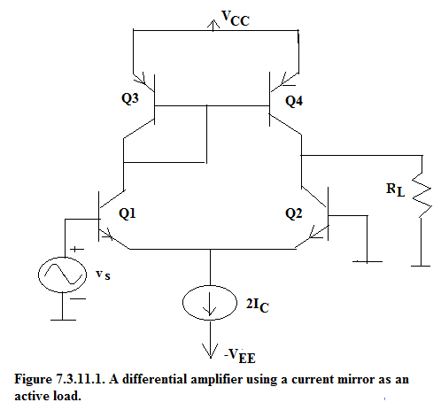
Here Q3 and Q4 constitute the Current Mirror. The two together act as the active load of the differential amplifier. Q1 and Q2 are the drivers of the differential amplifier. In exactly the same manner MOS can also be used as an active load .
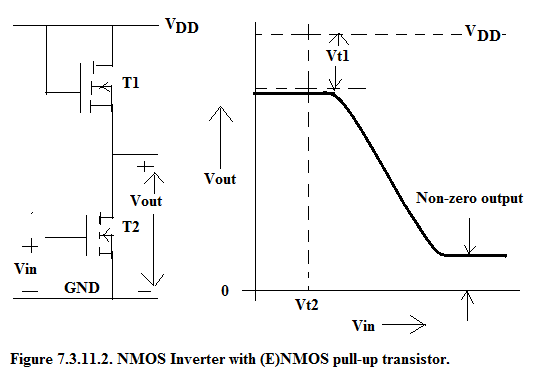
7.3.11.1. NMOS Inverter with (D)NMOS as pu transistor.
Passive load Pull-up configuration is technically unfeasible for IC technology. Hence we always go for Active Load Pull-Up configuration. The first configuration has already been discussed in Section 7.3.10. In this NMOS inverter with (D)NMOS as the Pull-Up transistor the biggest drawback is the standby power dissipation. When Vin = HIGH, Vout=LOW and both transistors are ON leading to rail to rail current flow hence power dissipated will be typically 5V×5mA = 25mW.
While switching the outut from ‘1’ to ‘0’, the actual switching starts when Vin has exceeded Vt [threshold voltage of (E)NMOS].
While switching the output from ‘1’ to ‘0’, load capacitance is rapidly discharged through the pd transistor which is in triode region. Pd transistor provides low resistance path hence time constant of discharge is short.
Similarly while switching from ‘0’ to ‘1’, load capacitance rapidly charges through pu transistor. Pu transistor also is in triode region for the latter part of switching from ‘0’ to ‘1’.
This is favourable feature which was encountered in Totem Pole configuration of TTL gates. This helps improve the switching speed but the standby dissipation under Vi = HIGH disfavours this circuit hence it was left out as IC Technology progressed.
7.3.11.2.NMOS Inverter with (E)NMOS as pu transistor
Figure 7.3.11.2 describes NMOS Inverter with (E)NMOS as pu transitor. Here also standby power dissipation is high when Vin= HIGH.
Vout never reaches V DD because of voltage equal to threshold voltage dropping along the channel.
By deriving V GG from a switching clock source, dissipation can be reduced. When Vin = HIGH we keep Gate of the active load LOW so that pu(T1) is turned off. So only driver (T2) is turned ON. T2 provides a low resistance path for the discharge of load capacitance when Vin = HIGH.
When Vin=LOW, T2 is OFF. During that period of Vin=LOW, we keep the gate of active load(T1) HIGH so that T1 is ON and low resistance path for charging the capacitive load. Hence Load Capacitance rapidly charges from ‘0’ to ‘1’ with a short time constant of charging.
This configuration is fast as well as it has low standby power but it has the added circuit complexity because of synchronized gate input of the active load. Hence this configuration has fallen into disfavour.
7.3.11.2.(E)NMOS Inverter with (E)PMOS as pu transistor- complementary transitor pull-up also known as CMOS Logic.
A NMOS Inverter with a (E)PMOS as pu transistor is shown in Figure 7.3.11.3. This complementary MOS configuration is known as CMOS. The permissible states are given in Table 7.3.11.1.
Table 7.3.11.1. The two permissible states of CMOS.
| (E)NMOS | (E)PMOS | Vout | ||
| Vin | LOW | OFF | ON(sourcing the current to the capacitive load) | HIGH(O/P has a low resistance path through ON PMOS to V DD ) |
| Vin | HIGH | ON(sinking the current from the capacitive load) | OFF | LOW(O/P has a low resistance path through ON NMOS to the GND) |
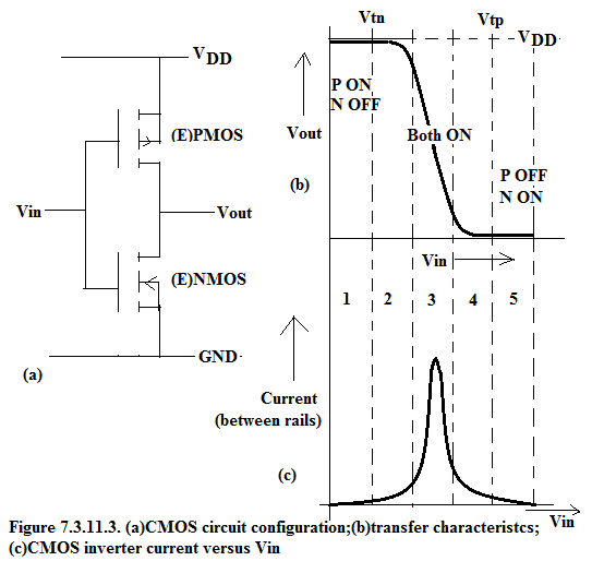
Part (a) of Figure 7.3.11.3 gives the circuit configuration, Part(b) gives the transfer characteristics and Part (c) gives the current flow.
In Part(b) we see that full logical levels are realized i.e. O/P HIGH=V DD and O/P LOW = 0V.
In Part (c) we see that under standby the current from rail to rail is zero. Hence standby dissipation is zero. Hence CMOS is also known as NanoWatt Logic.
During the switching there is a current flow from rail to rail hence dissipation per gate is directly proportional to clocking speed. In Figure 7.3.11.4 we compare the dissipation curves of TTL Logic and CMOS Logic under standby as well as under switching condition.
For identical geometries PMOS is slower than NMOS on account of lower mobility of holes. Hence to achieve identical switching time from LOW to HIGH and from HIGH to LOW, geometries will have to be optimized as we have to optimize for different configuration of NMOS inverter.

From here onward we will be focused on CMOS Logic and its analysis.
Notification Switch
Would you like to follow the 'Solid state physics and devices-the harbinger of third wave of civilization' conversation and receive update notifications?
|
|

|
|

|
|
|
|
|
|
|
|

|
|
|
|

|
|

|
|

|