

| << Chapter < Page | Chapter >> Page > |
SSPD_Chapter 7_part 4_CMOS lay-out design rules.
7.4.1. Introduction to VLSI Design.
Digital VLSI systems are mainly implemented by CMOS family of Logic in Silicon Wafer. Only for very high speed niche applications we go for ECL family of Logic. In this Chapter 7, we are mainly concerned with CMOS VLSI circuits. Figure 7.4.1 gives the flow chart of design and implementation of a CMOS Digital Systems.

7.4.2. Layout Design Rules.
As seen in Figure 7.4.1. from the designers layout the masks will be prepared and these masks will be translated into IC circuits in the foundry. These masks will be prepared within certain tolerances and with certain minimum resolutions. Mask preparation is the crucial step in IC technology and inorder that ICs are fabricated with high yield rate the tolerances and rsolutions must be clearly defined and hence layout design rules have been given.
Minimum wire widths are specified to avoid breaks. Minimum wire spacings are specified to avoid shorts. Overlaps are specified to ensure that overlap is complete. The design rules are expressed in terms of microns. The design rules are required so that a certain minimum resolution/tolerance of masks are permissible.
The Generation of the Fabrication Process technology is specified by the minimum feature size. Minimum feature size refers to channel length. As the Generation of the Fabrication Process advances so does the packing density and level of integration advances as shown in Table 7.4.1.
Table 7.4.1. Different Generations of Technology and their respective Packing Densities in Microprocessor Chips.
| Year | Chip | L | Transistors per cm square |
| 1971 | 4004 | 10µm | 2.3K |
| 1974 | 8080 | 6µm | 6.0K |
| 1976 | 8088 | 3µm | 29K |
| 1982 | 80286 | 1.5µm | 134K |
| 1985 | 80386 | 1.5µm | 275K |
| 1989 | 80486 | 0.8µm | 1.2M |
| 1993 | Pentium | 0.8µm | 3.1M |
| 1995 | Pentium Pro | 0.6µm | 15.5M |
| 1999 | Mobile PII | 0.25µm | 27.4M |
| 2000 | Pentium 4 | 0.18µm | 42M |
| 2002 | Pentium 4(N) | 0.13µm | 55M |
There are different design rules such as: Mead-Conway Design Rules, CUMF n-MOS Design Rules and Lambda based Design Rules. In this lecture we will concentrate on Lambda Based Design Rules.
1.Design rules are a set of geometrical specifications that dictate the design of the layout masks.
2.A design rule set provides numerical values:
3.Design rules must be followed to insure functional structures on the fabricated chip.
4.Design rules change with technological advances ( www.mosis.org ).
Design rules are classified as :Minimum width, Minimum spacing, Surround and Extension.
The following physical limitations compel us to specify the design rules:
Limits on N+ spacing:
If depletion regions of adjacent pn junctions touch, then

Figure 7.4.2. The depletion region surrounding N+ regions can merge hence a definite spacing has to be kept.
Electrical capacitive coupling can occur between closely spaced conducting lines. This leads to a problem called crosstalk
Hence closely spaced metal lines are kept well separated.
Certain electrical rules are followed such as the allowed width of a metal interconnect line:
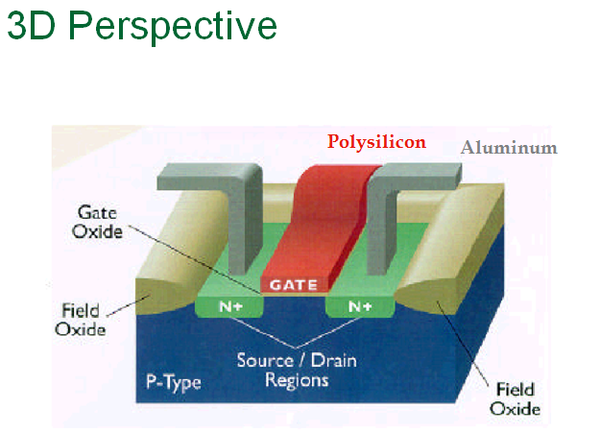
Figure 7.4.3. Three Dimensional Perspective View of NMOS fabricated in P-substrate.
Why do we use design rules?
The design rules provide the interface between designer and process engineer.
The design rules also provide the guidelines for constructing process masks.
Minimum length or width of a feature on a layer is 2lambda where lambda is half channel length. This is to allow for contraction of the feature.
Minimum separation of features on a layer is 2lambda.This is to ensure adequate continuity of the intervening materials.
Notification Switch
Would you like to follow the 'Solid state physics and devices-the harbinger of third wave of civilization' conversation and receive update notifications?

|
|

|
|

|
|

|
|

|
|

|
|

|
|

|
|

|
|

|