

| << Chapter < Page | Chapter >> Page > |
SSPD_Chapter 6_Part 4_concluded_MOS and its Physics.
What is an IDEAL MOS DIODE ?
The Band-Diagram of an Ideal MOS Diode is shown in Figure (A).

In an ideal MOS diode we have the following features:
In real MOS diode flat band voltage is not zero. There is always a difference between Metal Work-function and Semiconductor Work-function.
Consider an example of Metal (Al)-Oxide- P-typeSi as shown in Figure B:
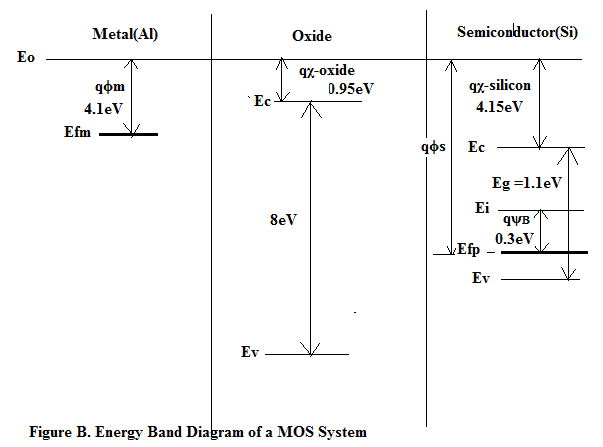
The Flat Band Voltage is = V FB = ϕm – ϕs = ϕm – [χ + E g /(2q) + ψ B ]
Therefore qV FB = qϕm – qϕs = qϕm – [qχ + E g /(2) + qψ B ] = 4.1 – [4.15+0.55+0.3]
Therefore qV FB = 4.1- 5.0 = - 0.9eV;
Because of this Flat-Band Voltage there is band bending even at zero gate voltage when gate and bulk are shorted. there is a depletion layer of negatively charged immobile Born ions just under the interface of SiO 2 /Si as shown in Figure C. Because of band-bending near the interface Si-bulk is more intrinsic hence holes are pushed out leaving behind the space-charge region. Negative electrons leave Gate Plate and recombine with the holes pushed out from the bulk. Therefore we get a dipole layer centered on the oxide layer as shown in Figure C. Negative voltage -0.9 eV when applied to the Gate of MOS system compensates for this band bending and flattens the Band Diagram as shown on the left side of Figure C. On the right side of Figure C we see that below the interface in the Si-bulk we have near-intrinsic semiconductor. In effect a depletion layer exists in the bulk under the interface. If the band bending is 2 qψ B then the depletion layer reaches its maximum width d max and when band bending exceeds 2 qψ B then an inversion layer is formed just under the interface in the bulk.

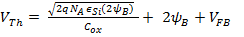
Theoretical Formulation of Threshold Voltage:
We will see in Chapter 6, Part 6, that the theoretical formula for thrshod voltage is given by:

Let us look at the ideal MOS diode in Figure A.
We have to apply sufficient gate voltage so the band bending at the interface is 2qψ B as shown in Figure D. This band bending is known as ‘Surface Potential Parameter’ = qψ S = 2qψ B . At this Gate to Source Voltage = V GS we have applied sufficient voltage to just cross the Threshold Voltage ‘V Th ’ and turn on the n-channel. The 2-D layer just below the Si-SiO 2 has experienced INVERSION. P-type semiconductor has been inverted to N-type semiconductor. The charges induced, the electric field created and the potential drop caused from Gate-to-Bulk is shown in Figure E.
.

As seen in Figure E, the charge on the Gate (Q G ) is exactly balanced by maximum depletion layer space-charge (Q dmax ) + inversion layer charge (Q i ).
That is Q G = (Q dmax + Q i )_______________________________ A.1
Because of electric flux lines originating on Q G and terminating on (Q dmax + Q i ) there is an uniform field in oxide layer E 0 and linearly graded E 1 just underneath the interface distributed across the depletion layer dmax wide.

Where W = width of the channel and L= length of the channel.

Q dmax is the space charge of the depletion layer ‘dmax’ wide.

The depletion layer of PN junction diode :

In MOS diode the depletion layer extnds in P-type bulk only and surface potential barrier (ψ S ) is equivalent to junction built-in potential barrier under no bias (ϕ BO ).
Assuming donor doping to be infinite and ϕ BO = ψ S equation A.4 reduces to:

When V GS = V Th then d p = dmax and

The space charge in depletion layer is:

Substituting A.6 in A.7 we get:

Referring to Figure E, in an ideal MOS Diode just at the point of turning ON:
V Th = V 0 + 2ψ B ;
Assuming Q G is equal to the space charge (Q dmax ) in dmax depletion layer with inversion layer weakly induced we have :

Substituting A.8 in A.9 we get:

We have already seen that Flat Band Voltage, V FB , has to be applied to flatten the band. This means a part of the job of the Gate Voltage is being done by V FB . Hence if this has to be accounted then Equation A.10 becomes A.11.
If source to bulk voltage (V SB ) is not zero then this also has to be accounted. This is called Body Effect. Now Equation A.11 becomes:

If the charges in Oxide layer and at Si-SiO 2 have to be accounted then
Q SS = Q it (interface trapped charges) + Q ot (oxide trapped charges) + Q m (mobile chares in the oxide) + Q f (fixed oxide charges) and Equation A.12 becomes:

This completes the theoretical formulation of the Threshold Voltage MOS device.
Notification Switch
Would you like to follow the 'Solid state physics and devices-the harbinger of third wave of civilization' conversation and receive update notifications?

|
|

|
|

|
|

|
|
|
|
|

|
|

|
|

|
|

|
|
|
|