

| << Chapter < Page | Chapter >> Page > |
SSPD_Chapter 6_Part 7_ Diode simulation Tutorial 1
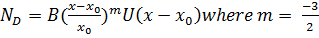
depletion width varies as the square root of the reverse bias voltage in step junction diode, varies as cube root of the reverse bias voltage in linearly graded junction diode and varies as the square of the reverse bias voltage in hyperabrupt junction diode where
m = -3/2. The varactor diode is used to assemble Voltage Controlled Oscillator (VCO) which is used in generating Frequency Modulated(FM) Carriers].

But at low currents (below 0.5mA) assumption (b) is violated and at high currents i.e at currents greater than 5mA assumption (a) is violated. In both cases :

Hence in diode equation :

Under two conditions, when I D is less tthan 0.5mA and greater than 5mA, V J = V D /2 and therefore real diode equation under these two conditions is:
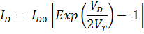
Therefore under these two conditions we have an Ideality Factor of η = 2 and real diode equation is given by:


| Type | Anode doping | Cathode doping |
| Conventionaldiode | 10 16 dopent atoms/cc | 10 16 dopent atoms/cc |
| Zener Diode | 10 19 dopent atoms/cc | 10 19 dopent atoms/cc |
| Backward Diode | 10 20 dopent atoms/cc | 10 20 dopent atoms/cc |
| Tunnel Diode | 10 21 dopent atoms/cc | 10 21 dopent atoms/cc |
Notification Switch
Would you like to follow the 'Solid state physics and devices-the harbinger of third wave of civilization' conversation and receive update notifications?

|
|

|
|

|
|

|
|

|
|

|
|

|
|

|
|

|
|

|