

| << Chapter < Page | Chapter >> Page > |
SSPD_Chapter 7_Device Simulation 3.
7.6. Simulation of BV CEO in BJT and determining the process parameters which control this device d.c. parameter namely Break-over Voltage or Sustaining Voltage.
go atlas
TITLE Bipolar BVCEO simulation
# Silvaco International 1994
mesh
x.m l=0 spac=0.1
x.m l=2 spac=0.1
y.m l=0 spac=0.002
y.m l=1 spac=0.10
region num=1 silicon
electrode num=1 name=emitter left length=0.8
electrode num=2 name=base right length=0.5 y.max=0
electrode num=3 name=collector bottom
doping reg=1 uniform n.type conc=5e15
doping reg=1 gauss n.type conc=1e18 peak=1.0 char=0.2
doping reg=1 gauss p.type conc=1e18 peak=0.05 junct=0.15
doping reg=1 gauss n.type conc=5e19 peak=0.0 junct=0.05 x.right=0.8
doping reg=1 gauss p.type conc=5e19 peak=0.0 char=0.08 x.left=1.5
save outf=bjtex05_0.str
tonyplot bjtex05_0.str -set bjtex05_0.set
# set poly emitter
contact name=emitter n.poly surf.rec
material taun0=5e-6 taup0=5e-6
# set models
models bipolar print
impact selb
solve init
method newton trap
solve prev
solve vbase=0.025
solve vbase=0.05
solve vbase=0.2
contact name=base current
method newton trap ir.tol=1.e-20 ix.tol=1.e-20
solve ibase=3.e-15
log outf=bjtex05.log master
# ramp collector voltage
solve vcollector=0.25
solve vcollector=0.5
solve vcollector=1
solve vcollector=3
solve vcollector=5
solve vstep=0.5 vfinal=10 name=collector compl=5.e-11 e.comp=3
# plot results
tonyplot bjtex05.log -set bjtex05_log.set
quit

Figure 7.12. The cross sectional view of the BJT being simulated.
The Tony Plot of the output curve for zero base current is shown in Figure 7.13. A real BJT under similar condition shows a ‘S’ type Negative Impedance Region(NIR) which is not being shown in the Tony Plot. BV CEO is shown to be around 8V.
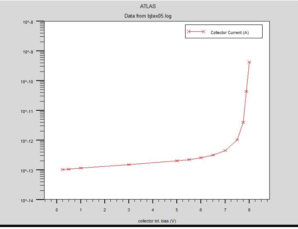
Figure 7.13. The output curve for base current zero.
7.6.1 Dependence of BV CEO on Base Width and Collector Base Doping.
As shown in Analog Electronics Lecture Notes,

As shown in SSPD notes for 2-sided step junction:

Where E critical = 3×10 5 V/cm for Silicon.
A shown in Analog Electronics Lecture Notes,
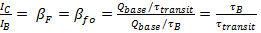
In Analog Electronics we have seen that transit time through the base:

Substituting Eq.7.6 in Eq.7.5 we get:

From Eq 7.3 it is clear the BV CEO ( the sustaining voltage of CE BJT) can be improved by increasing the Avalanche Breakdown Voltage of CB Junction and by decreasing short circuit current gain β fo .
From Eq. 7.4, it is evident that breakdown can be increased by making CB junction lighter doped. From Eq.7.7, it is evident that short circuit current gain can be reduced by increasing base width (W).
7.6.2. Increase in Sustaining Voltage through making CB junction lighter doped.
CB junction is not a double –sided step junction instead it is linarly graded junction where the following formula is applicable :

By equating E max = E critical we obtain the CB breakdown voltage as:

Here breakdown is critically dependent on ‘a’ = impurity gradient (1/cm 4 ). Therefore lowering of dopent concentration per se will not increase the sustaining voltage. We have to see how the change of dopent concentration effects the impurity gradient. Therefore lowering the dopent concentration is not tried out.
7.6.3. Increase in sustaining voltage by increasing the Base Width (W).

Figure 7.14. The Output Curve of BJT with Base Current zero and with Base Width increased.
In this case Base Width is increased from 1 micron to 1.2 micron by shifting BC Junction to 0.16micron and decreasing EB Junction to 0.04 micron. This has very clearly increased the sustaining voltage from 8V to 10V.
go atlas
TITLE Bipolar BVCEO simulation
# Silvaco International 1994
mesh
x.m l=0 spac=0.1
x.m l=2 spac=0.1
y.m l=0 spac=0.002
y.m l=1 spac=0.10
region num=1 silicon
electrode num=1 name=emitter left length=0.8
electrode num=2 name=base right length=0.5 y.max=0
electrode num=3 name=collector bottom
doping reg=1 uniform n.type conc=5e15
doping reg=1 gauss n.type conc=1e18 peak=1.0 char=0.2
doping reg=1 gauss p.type conc=1e18 peak=0.05 junct=0.16
doping reg=1 gauss n.type conc=5e19 peak=0.0 junct=0.04 x.right=0.8
doping reg=1 gauss p.type conc=5e19 peak=0.0 char=0.08 x.left=1.5
save outf=bjtex05_0.str
tonyplot bjtex05_0.str -set bjtex05_0.set
# set poly emitter
contact name=emitter n.poly surf.rec
material taun0=5e-6 taup0=5e-6
# set models
models bipolar print
impact selb
solve init
method newton trap
solve prev
solve vbase=0.025
solve vbase=0.05
solve vbase=0.2
contact name=base current
method newton trap ir.tol=1.e-20 ix.tol=1.e-20
solve ibase=3.e-15
log outf=bjtex05.log master
# ramp collector voltage
solve vcollector=0.25
solve vcollector=0.5
solve vcollector=1
solve vcollector=3
solve vcollector=5
solve vstep=0.5 vfinal=10 name=collector compl=5.e-11 e.comp=3
# plot results
tonyplot bjtex05.log -set bjtex05_log.set
quit
Notification Switch
Would you like to follow the 'Solid state physics and devices-the harbinger of third wave of civilization' conversation and receive update notifications?

|
|

|
|

|
|

|
|

|
|

|
|

|
|

|
|

|
|

|