

| << Chapter < Page | Chapter >> Page > |
SSPD_Chapter 6_Part 7_Device Simulation 2_concluded
7.5. Bipolar Gummel Plot with Ic/Vce with constant Ib
go atlas
TITLE Bipolar Gummel plot and IC/VCE with constant IB
# Silvaco International 1992, 1993, 1994
mesh
x.m l=0 spacing=0.15
x.m l=0.8 spacing=0.15
x.m l=1.0 spacing=0.03
x.m l=1.5 spacing=0.12
x.m l=2.0 spacing=0.15
y.m l=0.0 spacing=0.006
y.m l=0.04 spacing=0.006
y.m l=0.06 spacing=0.005
y.m l=0.15 spacing=0.02
y.m l=0.30 spacing=0.02
y.m l=1.0 spacing=0.12
region num=1 silicon
electrode num=1 name=emitter left length=0.8
electrode num=2 name=base right length=0.5 y.max=0
electrode num=3 name=collector bottom
doping reg=1 uniform n.type conc=5e15 # background doping of the N-epi layer
doping reg=1 gauss n.type conc=1e18 peak=1.0 char=0.2 # N-type Collector implant
doping reg=1 gauss p.type conc=1e18 peak=0.05 junct=0.15 #P-type Base implant;
doping reg=1 gauss n.type conc=5e19 peak=0.0 junct=0.05 x.right=0.8 #N-type Emitter implant;
doping reg=1 gauss p.type conc=5e19 peak=0.0 char=0.08 x.left=1.5 # base contact P-type implant;
# set bipolar models
models conmob fldmob consrh auger print# consrh means concentration dependent lifetimes applicable in Silicon. Print has been explained in Section 7.4.
contact name=emitter n.poly surf.rec # surf.rec means surface recombination.
solve init
save outf=bjtex04_0.str
tonyplot bjtex04_0.str -set bjtex04_0.set
# Gummel plot
method newton autonr trap
solve vcollector=0.025
solve vcollector=0.1
solve vcollector=0.25 vstep=0.25 vfinal=2 name=collector
solve vbase=0.025
solve vbase=0.1
solve vbase=0.2
log outf=bjtex04_0.log
solve vbase=0.3 vstep=0.05 vfinal=1 name=base
tonyplot bjtex04_0.log -set bjtex04_0_log.set
#IC/VCE with constant IB
#ramp Vb
log off
solve init
solve vbase=0.025
solve vbase=0.05
solve vbase=0.1 vstep=0.1 vfinal=0.7 name=base
# switch to current boundary conditions
contact name=base current
# ramp IB and save solutions
solve ibase=1.e-6
save outf=bjtex04_1.str master
solve ibase=2.e-6
save outf=bjtex04_2.str master
solve ibase=3.e-6
save outf=bjtex04_3.str master
solve ibase=4.e-6
save outf=bjtex04_4.str master
solve ibase=5.e-6
save outf=bjtex04_5.str master
# load in each initial guess file and ramp VCE
load inf=bjtex04_1.str master
log outf=bjtex04_1.log
solve vcollector=0.0 vstep=0.25 vfinal=5.0 name=collector
load inf=bjtex04_2.str master
log outf=bjtex04_2.log
solve vcollector=0.0 vstep=0.25 vfinal=5.0 name=collector
load inf=bjtex04_3.str master
log outf=bjtex04_3.log
solve vcollector=0.0 vstep=0.25 vfinal=5.0 name=collector
load inf=bjtex04_4.str master
log outf=bjtex04_4.log
solve vcollector=0.0 vstep=0.25 vfinal=5.0 name=collector
load inf=bjtex04_5.str master
log outf=bjtex04_5.log
solve vcollector=0.0 vstep=0.25 vfinal=5.0 name=collector
# plot results
tonyplot -overlay bjtex04_1.log bjtex04_2.log bjtex04_3.log bjtex04_4.log bjtex04_5.log -set bjtex04_1_log.set
quit
7.5.1. Discussion on the Atlas Program used for BJT Device simulation and characterization.
Below in Figure 7.6 and Figure 7.7, the implant profile of the dopents are given. Figure 7.6 gives the absolute doping profile and Figure 7.7 gives the net doping profile after compensation.
From Figure 7.7 it is clear that EB Junction is at 0.05µm and BC Junction is at 0.15µm. Emitter is heavily doped at 5×10 19 Phosphorous atoms per cc , Base is at 1×10 18 Boron atoms per cc and Collector is at the background doping of 5×10 15 Phosphorous atoms per cc. The base width is 0.10µm.
Figure 7.8 gives the mesh or the gridlines which cover the cross-sectional area of the device. As seen from the Mesh Diagram it is 0 to 1 µm in vertical or Y-direction and 0 to 2 µm in lateral direction or in X-direction.
As seen from Figure 7.8, finest mesh covers the encircled area and second finest mesh covers the bracketed are.
In Figure 7.9, 7.10 and 7.11 the Tony Plot of the structure of vertical NPN, I C and I B with respect to V BE and family of output curves (I C vs V CE ) are given respectively. Not in Figure 7.9 we see that ratio of I C and I B for constant V CE is the short circuit d.c. current gain, β F , which is poor at low currents due to recombination in the depletion layer and it is also poor at large currents due base conductivity modulation. It is optimum around 100 at I C = 0.5 to 5mA. Emitter Injection Efficiency is degraded due to recombination in depletion layer and due to base conductivity modulation.

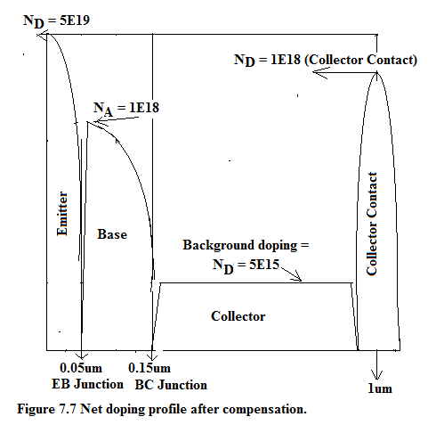

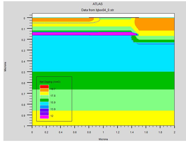
Figure 7.9. The structure generated by Tony Plot.
Figure 7.10. Variation of Base and Collector Current keeping Vce constant. The ratio of the two will give short circuit current gain . Note that at low currents β is unity and this gain plateaus at 5mA and at high current it again falls.
Figure 7.11. Output family of curves I C -V CE for the given transistor under constant current drive.
Notification Switch
Would you like to follow the 'Solid state physics and devices-the harbinger of third wave of civilization' conversation and receive update notifications?

|
|

|
|

|
|

|
|

|
|
|
|
|
|
|
|
|
|
|

|
|

|