

| << Chapter < Page | Chapter >> Page > |
AnalogElectronics_Lecture3supp._High Frequency Model of PN Junction Diode.
At high frequency, the Depletion Layer Junction Capacitance(C JD ) under reverse biased and {C JD plus C D (Diffusion Capacitance)} comes in parallel with the incremental resistance r d . At very high frequencies even the leads will offer an inductive reactance but we are going to neglect it for the present syllabus. The incremental Model of PN Junction Diode at high frequencies is given in Figure 1.
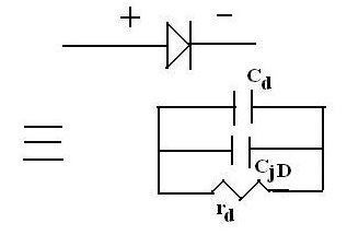
Figure 1. Incremental Model of Diode at high frequencies.
Junction Capacitance (C jD ) is present in both reverse and forward biased diodes because it is due to depletion layer/space charge layer/dipole layer present at the metallurgical junction of the diode.
Diffusion Capacitance(C d ) is present only in forward bias because it is due to excess minority carrier stored under forward biased condition. In reverse bias condition there is no excess minority carrier stored in the bulk region.
In Figure 2 we see the deleterious effect of C d + C jD on the switching performance of the diode. Ideally a diode should stop conducting and it should switch off but this switch off is not instantaneous. If a forward biased diode is reverse biased it continues to conduct in the reverse direction for time (t storage + t discharge ) before it switches off. The switching transient of a diode is shown in Figure 2.
The delay in switching is due to the time delay in removing the excess minority carriers and time taken in discharging the junction capacitance.
Time delay in removing the minority carriers is storage delay = t storage ;
Time taken in discharging the junction capacitance shows up as a fall time = t discharge ;
The Physics of removal of minority carriers and discharging of C JD are shown in Figure 3.

Figure 2.Switching Transient of a Diode.

Figure 3. The process of minority carrier removal during (t storage + t discharge )
Diode Junction Capacitance (CjD) = (ε 0 ε r A/d) where A= cross sectional area of the diode and d=depletion width;
Physics of Diode Junction Capacitance:
The doping profile of N+ and P- decide the voltage dependence of Junction Capacitance.

Figure 4. Doping profile of abrupt junction, linearly graded junction and hyper-abrupt junction.

z 0 = position of metallurgical junction along the longitudinal axis.
Depletion Width in a hyper-abrupt junction:
d~ d p = K(V R ) 1/(m+2)

In an abrupt junction or one sided step junction, m = 0 :

In linearly graded junction, m = 1:

In hyper - abrupt junction, m = -


Hyper - abrupt Junction Diode is known as VARACTOR DIODE. It is used for Frequency Modulated Waves generation.

Figure 5. Arrangement for modulating Varactor diode junction capacitance by audio signal.

Figure 6. A Colpitts Oscillator with a varactor diode in its tank circuit.
The frequency of oscillation of Colpitts Oscillator is the Frequency of Resonance of the Tank Circuit.
Radial Frequency of Oscillation=ω
0 =

Let C
j /C
0 >>1 then ω
0 =

Therefore ω
0 =

Thus we obtain frequency proportional to frequency. This generates FM carrier.
Physics of Diffusion Capacitance:
It can be shown that diffusion capacitance C d can be obtained by the following relation:
For one sided step junction N+P,
r d C d = τ n where τ n life-time of minority carriers in lightly doped side.
In equally doped diode,
1/ r d C d = 1/τ n + 1/τ p where τ n life-time of minority carriers on P-type doped side.
τ p life-time of minority carriers in N-type doped side.
In BJT in forward active mode:
r e C d = τ t
where r e = incremental resistance of EB diode;
τ t = transit time across the base.
Notification Switch
Would you like to follow the 'Solid state physics and devices-the harbinger of third wave of civilization' conversation and receive update notifications?

|
|

|
|

|
|
|
|
|

|
|

|
|

|
|

|
|

|
|
|
|