

| << Chapter < Page | Chapter >> Page > |
SSPD_Chapter 3_Section 3.2.3.Theoretical Formulation of the Knee Voltage(V γ ) of a forward biased-diode.
In Section 3.2.2. we have derived the Ideal Diode Equation:

We choose the fabrication parameters of a typical Diode as given in Table 3.2.2.3. They are as follows:
Wide-Bulk diode with N-Type Doping 10 16 /cc and P-Type Doping 10 18 /cc and life-time τ n = τ p =1μs, cross-sectional area A= 10 -3 cm 2 .
D n (on P-side)= 7.3cm 2 /s; L n (on P-side)=0.27μm;
D p (on N-side)= 7.8cm 2 /s; L p (on N-side)=0.279μm;
Therefore I D =I D0 [λ-1] where λ=Exp(V F /V Th );
Substituting the fabrication parameters we get:
I D =I D0 [λ-1]=4.5×10 -13 [λ-1]Amp.
Let us define the knee voltage of a forward biased diode as the forward bias at which 10μA flows through the diode. Hence Ideal Diode Equation is:

Since Thermal Voltage is 26mV and Knee Voltage will be several times greater than V Th therefore Equation 3.2.3.1 reduces to:

Thermal equilibrium value of minority carrier can be replaced by (n i 2 /dopent density). Equation 3.2.3.2 becomes:

Replacing n i 2 by its theoretical form given in Equation(3.2.11) we get:

Substituting the fabrication and electrical parameters we get:
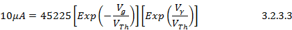
Equation (3.2.3.3) simplifies to :

Taking the natural log of Equation (3.2.3.4):

Therefore V γ =V g – 24.53×V Th = V g – 0.6379 ______________________________ 3.2.3.6.
The Knee Voltages of Ge, Si and GaAs at 300K are tabulated in Table 3.2.3.1.
Table 3.2.3.1.Knee Voltages of Ge,Si and GaAs diodes at 300K frpm Equation (3.2.3.6)
| Material | Band-Gap Voltage(V) | Knee Voltage(V) |
|---|---|---|
| Ge | 0.67 | 0.03 |
| Si | 1.12 | 0.482 |
| GaAs | 1.4 | 0.7621 |
By observation the knee voltages observed for the three diodes are of the same range as given in the Table. From Equation (3.2.3.6) we see that knee voltage is determined by material Enegy Band Gap Voltage.
Notification Switch
Would you like to follow the 'Solid state physics and devices-the harbinger of third wave of civilization' conversation and receive update notifications?

|
|

|
|

|
|

|
|

|
|

|
|

|
|

|
|

|
|

|