

| << Chapter < Page | Chapter >> Page > |
We then remove the remaining resist, and perform an activation/anneal/diffusion step, also sometimes called the"drive-in". The purpose of this step is two fold. We want to make the n-tank deep enough so that we can use it for ourp-channel MOS, and we want to build up an implant barrier so that we can implant into the p-substrate region only. Weintroduce oxygen into the reactor during the activation, so that we grow a thicker oxide over the region where we implanted thephosphorus. The nitride layer over the p-substrate on the LHS protects that area from any oxide growth. We then end up withthe structure shown in [link] .

Now we strip the remaining nitride. Since the only way we can convert from p to n is to add a donor concentration which isgreater than the background acceptor concentration, we had to keep the doping in the substrate fairlylight in order to be able to make the n-tank. The lightly doped p-substrate would have too low a threshold voltage for goodn-MOS transistor operation, so we will do a adjust implant through the thin oxide on the LHS, with the thick oxide on the RHS blocking the boron from getting intothe n-tank. This is shown in [link] , where boron is implanted into the p-type substrate on the LHS, but isblocked by the thick oxide in the region over the n-well.

Next, we strip off all the oxide, grow a new thin layer of oxide, and then a layer of nitride [link] . The oxide layer is grown only because it is bad to grow Si 3 N 4 directly on top of silicon, as the different coefficients ofthermal expansion between the two materials causes damage to the silicon crystal structure. Also, it turns out to be nearlyimpossible to remove nitride if it is deposited directly on to silicon.
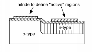
The nitride is patterned (covered with photoresist, exposed, developed, etched, and removal of photoresist) to make two areaswhich are called "active" [link] . The wafer is then subjected to a high-pressure oxidation step which grows a thick oxide whereverthe nitride was removed. The nitride is a good barrier for oxygen, so essentially no oxide grows underneath it. The thickoxide is used to isolate individual transistors, and also to make for an insulating layer over which conducting patterns canbe run. The thick oxide is called field oxide (or FOX for short) [link] .

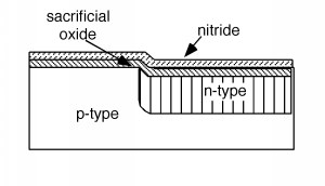
Then, the nitride, and some of the oxide are etched off. The oxide is etched enough so that all of the oxide under thenitride regions is removed, which will take a little off the field oxide as well. This is because we now want to grow thegate oxide, which must be very clean and pure [link] . The oxide under the nitride is sometimes called a sacrificial oxide , because it is sacrificed in the name of ultra performance.
Notification Switch
Would you like to follow the 'Chemistry of electronic materials' conversation and receive update notifications?

|
|

|
|

|
|

|
|

|
|

|
|

|
|
|
|
|

|
|

|