

| << Chapter < Page | Chapter >> Page > |
j is the quantum number which describes the level of modulation.
In Figure(1.47), we describe three matter waves: ψ 11 , ψ 21 , ψ 41 . In Figure 1.48 we show matter wave ψ 42
For simplicity of description we have assumed linear array of 4 lattice centers i.e.
L= 4a;
We have seen in Part 8_conclusion that at a step voltage there is a reflected wave. When two reflected waves constructively interfere we have a condition of Bragg Reflection or Specular Reflection. Under this condition forward and reflected wave cancel each other and electron does not exist as a physical entity. Hence the energy states corresponding to this Brag Reflection is forbidden.
Constructive Interference occurs when:
Path difference of two normally incident waves = 2a = nλ as we saw in x-ray crystallography.
Destructive Interference occurs when:
Path difference of two normally incident waves = 2a = (n+1/2) λ;
Therefore when the wavelength of matter wave satisfies the condtion:
λ = 2a/n................. 1.88.
That particular wavelength electron suffers Bragg Reflection.
Bragg reflection was discussed in context of matter wave and its experimental verification of matter wave in Chapter 1_Part 3. Bragg had done X-Ray diffraction using crystalline grating and Davisson-Germer had done electron diffraction again using crystalline grating.
The wave vector of matter wave is : k z = 2π/λ;
Substituting Eq.(1.88) in wave vector we get:
k z = (π/a)n................... 1.89
Equation 1.89 implies that electrons in a crystalline lattice will not exist at k z equal to :
±(π/a)1 , ±(π/a)2 , ±(π/a)3 , ±(π/a)4 ……..
Bragg brothers had received the Nobel Prize for demonstrating the mirror like reflection or specular reflection of X-Rays from crystal surfaces as described in Chapter 1_Part 3.
From Equation (1.88) and Equation (1.89) we see that matter wave does not exist due to Bragg Reflection and discontinuity is created at those points:
The points of discontinuity:
| Points of discontinuity in E-k diagram at k n | k 1 = π/a | k 2 = 2π/a | k 3 = 3π/a | k 4 = 4π/a |
| But k n = 2π/λ n therefore λ n of the matter wave | λ 1 = 2a | λ 2 = a | λ 3 = 2a/3 | λ 4 = a/2 |
| In terms of principle quantum number nWhere L= 4a | nπ/L = π/a | nπ/L=2π/a | nπ/L=3π/a | nπ/L=4π/a |
| Principle quantum number | 4 | 8 | 12 | 16 |
| Corresponding Wave Function | ψ 4,1 | ψ 8,1 | ψ 12,1 | ψ 16,1 |
This implies that these matter waves will not exist. Therefore matter waves at wave vectors : ± (π/a), ± (2π/a) , ± (3π/a) , ± (4π/a), ………
do not exist because they suffer specular reflection or Bragg Reflection.
At these wave vectors of discontinuity, different levels of modulation contribute to bands of energies at wave vectors ± (π/a), ± (2π/a) , ± (3π/a) , ± (4π/a), ………
Hence the non-existence of the matter waves at these points of Bragg Reflection lead to band gaps in otherwise continuous energy distribution with respect to wave vector. Hence continuous E- k diagram shown in Fig(1.45) becomes Energy Band diagram alternated by Energy Gaps as shown in Fig(1.49). The Energy Band Gaps are also referred to as Forbidden Band Gaps.

Figure(1.49) Energy Band Diagram of electrons in a single crystal solid.
Through the above discussion we have established qualitatively that electrons in a single crystal solid occupy permissible bands of energy alternated by forbidden band gaps.
Solid State Band Theory has introduced us to a new quantum mechanical phenomena called Bragg reflection.
We have seen that at k= ± (π/a), ± (2π/a) , ± (3π/a) , ± (4π/a),……..
electrons suffer specular reflection which does not permit the independent existence of electrons at those wave vectors or at those momenta vectors since p= kћ. If we closely examine E-k diagram at the discontinuities we see that E-k curve does not follow the parabolic relationship as it does elsewhere. Hence the behavior of electron at the discontinuities is quite different from its behavior elsewhere. To examine the behavior at the discontinuities we will have to re-examine the Schrodinger Equation in spatial coordinates:
∂ 2 ψ/∂z 2 + [{2m(E-V(z))}/ћ 2 ]ψ = 0................ 1.90
V(z) is the periodic potential variation;
In an infinite crystal with a period of L = Na where a is the lattice parameter the solution is a progressive wave:
Namely ψ(z,t)= ψ 0 (z)Exp[j(ωt-kz)]
Where k = √[2m{E-V(z)}]/ћ
Therefore E= ћ 2 k 2 /(2m e ) + V(z);
If we assume an effective mass m e * which incorporates the periodic potential variation in itself then we get an expression:
E = ћ ^2 k ^2 /(2m e * )............. 1.91
Double differential of E with respect to k gives us the expression of the effective mass:
m e * = ћ ^2 /(∂ 2 E/∂ 2 k)............... 1.92
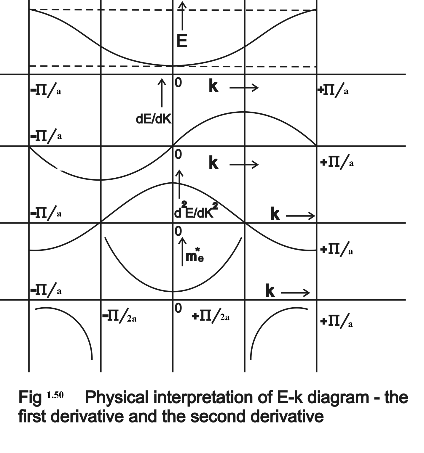
Figure 1.50. Physical interpretation of E-k diagram.
The following conclusions result from the inspection of the E-k diagram and its derivatives:
Therefore effective mass is fully dependent on E-k relationship. In Figure(1.50) the first derivative and the second derivative are given. As seen from the diagram, near the lower band edge the second derivative ∂ 2 E/∂ 2 k is higher than the normal value hence at the lower band edge effective mass is lighter than the free space mass. At the upper edge ∂ 2 E/∂ 2 k is negative hence mass is negative . This gives rise to the phenomenological particle called holes. Holes are the movement of vacancies.
Band theory illustrates a new property of electron namely the property of scattering which is responsible for the resistivity of a conducting solid. Next chapter is devoted to scattering of electrons and resistivity.
Table 1.9 The effective mass m e * of conducting electrons in different metals.
| Metal | Ag | Au | Bi | Cu | K | Li | Na | Ni | Pt | Zn |
| m e * /m e | 0.99 | 1.1 | 0.047 | 1.01 | 1.12 | 1.28 | 1.2 | 28 | 13 | 0.85 |
Notification Switch
Would you like to follow the 'Solid state physics and devices-the harbinger of third wave of civilization' conversation and receive update notifications?

|
|

|
|

|
|

|
|

|
|

|
|

|
|

|
|

|
|

|