<< Chapter < Page Chapter >> Page >

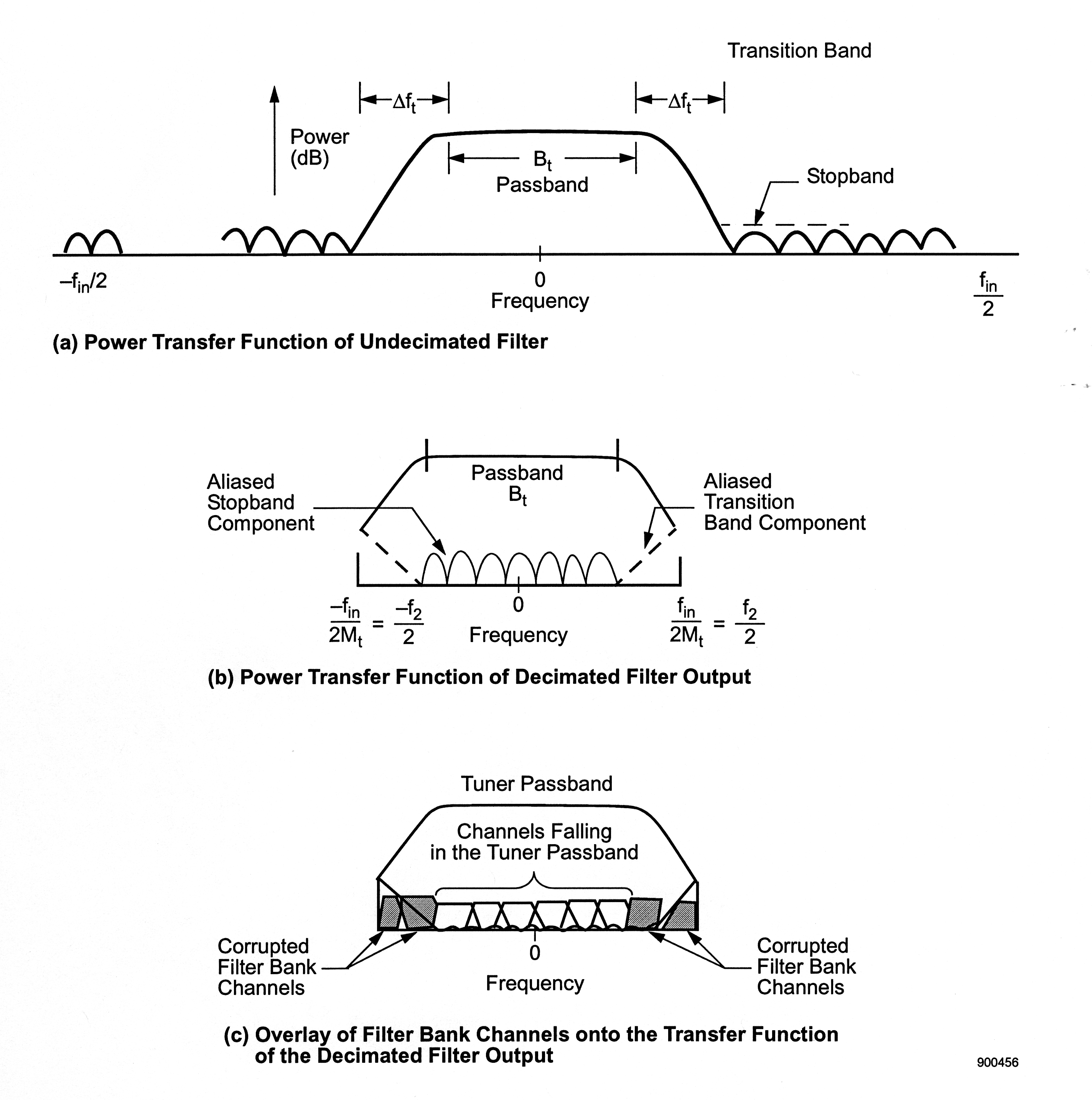
One implication of f s being significantly larger than B t is that many of the channels or filters in the transmux-based filter bank are not useful. To visualize this, consider [link] . [link] (a) shows the power transfer function of the tuner filter before its output is decimated to the rate f s . The passband of the filter is B t Hz wide, the transition band on each side of the passband is Δ f t Hz wide, and the stopband extends from B t 2 + Δ f t Hz to the Nyquist folding frequency f i n 2 . [link] (b) shows the power transfer fumction of the decimated filter. In this case, we assume that the transition band Δ f t is slightly less than f s - B t . With this choice, some energy passed by the tuner through the transition bands folds back into the output, but none falls in the passband. [link] (c) shows the channels of the transmux-based filter bank overlaying the tuner's power transfer function. The channels falling within the passband are clean, that is, the tuner's passband ripple and stopband rejection apply there, but the channels falling in the transition band are subject to several degradations (for example, gain slope and out-of-band signal aliasing) and are therefore not useful in most cases. Thus even though the transmultiplexer breaks the f s Hz band at the output of the tuner into N channels, only C of them, where C = B t Δ f = N · B t f s , are typically used for downstream processing.

Hardware examples of tuner/transmux tradeoffs

This company has built a number of digital transmultiplexers for various applications and all of them employ some form of digital tuner. The next three sections present a few of these designs with the intent of demonstrating how the overall system design decisions were made.

A single-card supergroup tuner/transmux

As a part of an IR&D program, the company developed an FDM supergroup transmultiplexer during 1985. Its basic requirements were to accept an FDM supergroup (that is, 60 voice grade channels spaced at regular intervals of 4 kHz over a band of 240 kHz) located at any of several possible spectral bands. These bands include 2-242 kHz, 12-252 kHz, 60-300 kHz, 312-552 kHz, and 564-804 kHz. Another key goal was excellent technical performance. To achieve this, the transmultiplexer portion was designed to use 16-bit arithmetic and key design parameters of f s = 4 kHz, K = 1 , and Q = 16 .

Since a supergroup only occupies 240 kHz, a convenient choice of f s would be 256 kHz. This value exceeds 240 kHz and makes N equal 64, an integer power of two and four. This value proves not to be globally optimum, however, as we will see after examining the tuner's requirements.

Figure three contains three parts. Part as is a graph titled, Power Transfer Function of Undecimated Filter. It consists of a series of plotted waves on a horizontal axis that ranges in Frequency from -f_in/2 to f_in/2  The waves begin from left to right with two small waves that both begin and end on the horizontal axis. There is then a break in the graph, and a new wave begins a portion towards the right. The new wave follows the shape of the previous waves, but one quarter of the wave where it would have began on the horizontal axis looks like it has been erased. There are four small waves in this section, with an arrow above them labeled Power (dB). After the small waves is one large wave, approximately 5 times the amplitude and 8 times the wavelength of the smaller waves to its left and right. The large wave has a long, wide peak. The width of the increasing portion of the wave before it reaches its peak is labeled ∆f_t. The width of the peak is measured as B_t passband. The width of the decreasing portion of the wave is measured as ∆f_t. After the large wave are six more small waves, this time with amplitude measured as stopband. Part b is titled Power Transfer Function of Decimated Filter Output. It consists of a series of waves plotted along a horizontal frequency axis that ranges in value from  -f_in/2M_t=-f_2/2 to f_in/2M_t = f_2/2. In the middle of the graph are seven waves with small amplitude and uneven shape. An arrow points at these waves, labeling them Aliased Stopband Component. Above these waves is a larger wave similar to the large wave in part a, with a wide peak. The width of the peak is measured and labeled as Passband B_t. The figure is not drawn to be wide enough to fit the entire large wave, and so it is cut off at the edge points at some vertical value above the peaks of the smaller waves. From the edge of the waves, which do not reach the edge of the figure, there are dashed diagonal lines connected to the edge of the larger wave. Part c is titled Overlay of Filter Bank Channels onto the Transfer Function of the Decimated Filter Output. The shapes in this part look roughly similar to part b, except that the small waves have wide peaks and overlap, and they extend to the edge of the figure, with the excess waves beyond what existed previously now shaded grey. The small waves are labeled Channels Falling in the Tuner Passband. The grey shaded area is labeled Corrupted Filter Bank Channels, and the large wave is labeled Tuner Passband.
The Impact of the Tuner's Transition Bandwidth on the Number of Useful Filterbank Outputs

The highest input frequency of interest to the tuner is 804 kHz. The sampling rate must therefore exceed this value by two or more. The actual rate chosen was 2.048 kHz. This was based on several considerations:

  • It satisfies the Nyquist sampling theorem and includes some allowance for the imperfections of analog antialias filtering.
  • It is a power-of-two integer multiple of Δ f = 4 kHz.
  • It was the highest sampling rate attainable with financially acceptable 12-bit A/D converters of the era. Twelve-bit digitization was desired to maximize the unit's noise power ratio (NPR) and dynamic range.

Get Jobilize Job Search Mobile App in your pocket Now!

Get it on Google Play Download on the App Store Now


Source:  OpenStax, An introduction to the fdm-tdm digital transmultiplexer. OpenStax CNX. Nov 16, 2010 Download for free at http://cnx.org/content/col11165/1.2
Google Play and the Google Play logo are trademarks of Google Inc.

Notification Switch

Would you like to follow the 'An introduction to the fdm-tdm digital transmultiplexer' conversation and receive update notifications?

Ask