

| << Chapter < Page | Chapter >> Page > |
Section 5.4. Nano-Size Effect on various opto-electronic-magnetic properties of nano materials.
A nano-particle or a Quantum Dot Semi-conductor ‘Si’ is a cluster of large number of atoms arranged in the minimum energy configuration. If the there are N atoms there are about N electrons or a few times more in this cluster. Most of these electrons are tightly bound to their host atoms. But there are few carriers electrons and holes which behave like particles in an infinite potential well. The scenario is depicted in Figure 5.12a. These behave just as electrons behave in isolated Hydrogen Atoms. Hence Quantum Dots are Artificial Atoms.

The Schrodinger equation of a particle in an infinite potential well is:

In Quantum Mechanics we have canonical variables: x and p or t and E.
Linear Momentum ‘p’ is equivalent to an operator:

Therefore Schrodinger Equation for a particle in an infinite potential well is:

Hamiltonian Operator operates on Matter Wave ψ to yield the eigen value of energy E. (5.4.1) simplifies to Second Order Ordinary Linear Differential Equation with two arbitrary constants determined by the two boundary conditions namely:

The simplified Schrodinger Equation is:

The Solution is Complementary Function:

With the given two boundary condition (5.4.3) simplifies to:

To satisfy the given boundary condition:

If V = 0 then the discrete energy states occupied by a carrier in an infinite 1-D Potential Well are:

The energy separation between two adjacent energy states is:

The actual energy states in a semiconductor are:

In Equation 5.4.8., L is the Radius of the Quantum Dot. By adjusting the size (i.e. R) of the Quantum Dot, it is continuously tunable through all the seven colours of a Rainbow.
The delocalization of electrons and structural changes in nano materials causes band-gap energy change in semi-conductor nano materials as well as changes in the following properties:
i.Optical properties,
ii.Melting Point,
iii.Specific heat,
iv.Surface reactivity,
v. Magnetic Properties,
vi.Electrical conduction.
Table 5.2. gives the Specific Heat of Palladium, Copper and Rubidium in bulk-size and in nano-size.
Table 5.2. Specific Heat of Pd,Cu and Ru in bulk and in nano-size.
| Elements | Bulk(J/(mol.K)) | Nano(J/(mol.K)) | Nano-size | %increase |
|---|---|---|---|---|
| Pd | 25 | 37 | 6nm | 48 |
| Cu | 24 | 26 | 8nm | 8.3 |
| Ru | 23 | 28 | 6nm | 22 |
As the bulk-size moves to nano-size, the Melting Point reduces as given below:


In Figure 5.13 it is shown that M.P. of gold particles decreases dramatically as the particle size gets below 5nm.
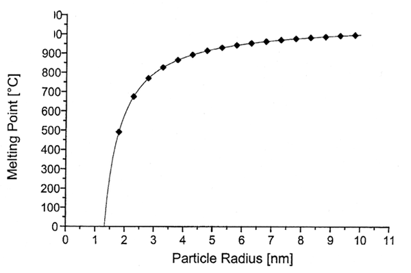
Figure 5.13.M.P. of Gold Particles vs Particle Size.

Figure 5.14. Quantum Dots of smaller size emit shorter wavelengths.
QD comprises of million atoms and equivalent valence electrons. But QD does have a few free electrons. These electrons behave like particle in an Infinite Potential Well. The Schrodinger Equation has been solved in m33488. That solution tells us electron occupies discrete energy states given by the following equation:


From (2) it is clear that smaller the dot size larger, larger will be the energy packet absorbed during excitation or larger will be the energy packet radiated when Dot settles to ground state. This is the reason why in Figure 5.14 as the dot size decreases it is seen to emit shorter wavelengths This emission can be LASER type coherent emission or LED type incoherent emission.
Confining a carrier in atleast one spatial dimension at the scale of the order of de Broglie Wavelength leads to Quantum Size Effect.
In Bulk - 3 degrees of freedoms with 0 degreeof Quantum Confinement. So we get bands of permissible energy.
In Quantum Well – 2 degrees of freedom with 1 degree of Quantum Confinement. .
In Quantum Wire - 1 degree of feedom and 2 degrees Quantum Confinement.
In Quantum Dot – 0 degree of freedom with 3 degrees of Quantum Confinement.
Hence in a Quantum Dot, electron behaves as an electron in infinite 1-D Quantum Well. Hence electron behaves as it behaves in a Hydrogen Atom and carriers have discrete energy states. Therefore QD is referred to as an artificial atom.
QD are extremely small semiconductor structures ranging from 2nm to 10nm. At these small dimensions, materials behave differently giving QD unprecedented tunability and enabling never before seen applications in Science&Technology.
The Band-gap of nano-structure:

QD LEDs can produce any colour including white light, it is extremely energy efficient giving the highest Lumens per Watt (uses only few watts) whereas CFL uses more than 10W. Its lifetime is 25 times that of incandescent lamp. But these are expensive . As its price falls due high demand and mass-production, these will become affordable.
Section 5.4.1. Electrical Conduction.
In bulk metal, current flow is according to Ohm’s Law:


In nano-material, band theory does not hold good so Ohm’s Laws is no longer applicable and special transport equations have to be formulated for accounting for the tunnel currents from nano-particle to nano-particle.
Section 5.5. Electric and Magnetic Properties of matter.
Electron is responsible for two distinct properties:
1- Charge ->It gives all electrical properties of mater.
Conductivity, Paraelectric, ferroelectric, antiferroelectric, diaelectric etc.
2- Spin->It gives magnetic properties.
Paramagnetic, Ferromagnetic, Antiferromagnetic, Diamagnetic, superparamagnetic, Ferrimagnetic, Canting magnetism, Superferromagnetism.
5.5.1.Charging Energy of nano-particle.
Capacitance of a Sphere is:

Therefore charging energy U for nanoparticle of radius a is:

This is 10 times larger than thermal energy at Room Temperature of 300K which is 25meV.
25meV corresponds to the charging energy of a nano-particle of radius 14.4nm.
So we conclude there is considerable charging energy for nano particle.
5.5.2. Density of States.
It can be shown that Density of permissible Energy States is as follows:


Pictorially it is shown in Figure 5.16

Notification Switch
Would you like to follow the 'Electrical and electronic materials science' conversation and receive update notifications?

|
|

|
|

|
|

|
|

|
|

|
|
|
|
|
|
|
|

|
|

|