

| << Chapter < Page | Chapter >> Page > |
As indicated in [link] , pulses are initiated at intervals of seconds, and each is scaled by the 4-PAM symbol value. This translates the discrete-time symbol sequence (composed of the messages interleaved with the preamble) into a continuous time signal
The actual transmitter symbol period is required to be within some tolerance of the nominal symbol period , but the Transmitter allows the introduction of a non-ideal clock that is slightly different from the specified (true)clock at the receiver. The transmitter symbol period clock is assumed to be steady enough that the timing offset and its period are effectively time-invariant over the duration of a single frame.
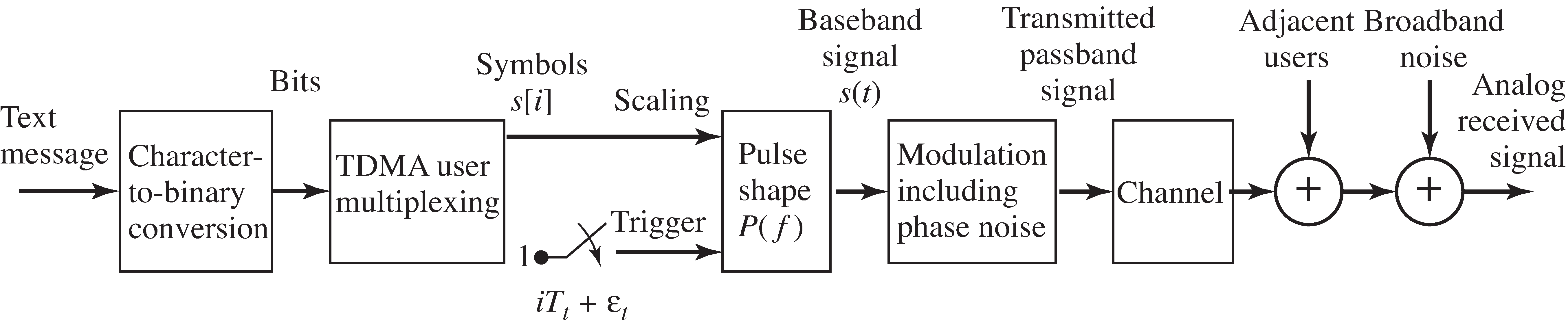
The pulse-shaping filter is a square-root raised cosine filter symmetrically truncated to a specified number ofsymbol periods. The rolloff factor of the pulse-shaping filter is fixed within some range and is known at the receiver,though it could take on different values with different transmissions. The pulse-shaped signal is then converted to theRF frequency and passed through the channel. Since the receiver is assumed to employ a sampled IF architecture,the IF frequency completely specifies the behavior of the signal in the frequency domain.While it might seem preferable to build a transmitter that operates at the RF frequency to more accurately model the real transmitter, the number of samples necessary to represent such a signal is large enough that it is rarely desirable.
The channel may be near ideal, i.e. a unit gain multi-symbol delay, or it may have significant intersymbol interference. In addition it can be time-varying, and the code allows two ways to introduce time variation. The first permits specification of the channel impulse response at the start of the transmission and the channel impulse response at the end of the transmission. At any time in between, the actual impulse response moves linearly from to . The second method of introducing time variation is to model the channel variation as a random walk. The variance of therandom walk process can be specified. In either case, the impulse response of the channel is unknownat the receiver, though an upper bound on its delay spread may be available in practice.There are also other disturbances which may be present, including interference from adjacent channels and narrowband interferers.These disturbances can also be controlled using the Transmitter, and they are assumed to be unknown at the receiver.
The achieved intermediate frequency is required to be within some user-specified tolerance of its assigned value.The carrier phase is unknown to the receiver and may vary over time, albeit slowly, due to phase noise.This means that the phase of the intermediate frequency signal presented to the receiver sampler may also vary.
The frontend of the sampled IF receiver, as shown in [link] , consists of a low noise amplifier, a preselect filter, AGC, mixer for downconversion to IF, and the sampler. The preselect filter partially attenuates adjacentFDM user bands. The automatic gain control is presumed locked and fixed over each transmission, and outputs a signalwhose average power is unity. The free-running sampler frequency needs to be well above twice the baseband bandwidth of the user of interest to allow proper functioning of thebaseband analog signal interpolator in the DSP timer in the the receiver. However, need not be twice the highest frequency of the IF signal. This implies that the sampled received signal hasreplicated the spectrum of the user transmission at the output of the front-end analog downconverter lowpass filter to frequencies betweenzero and IF.
Notification Switch
Would you like to follow the 'Software receiver design' conversation and receive update notifications?

|
|

|
|

|
|

|
|

|
|

|
|

|
|

|
|

|
|

|