

| << Chapter < Page | Chapter >> Page > |
Empirical equations can be determined by fitting experimental data of extinction coefficient per mole of Group 12-16 semiconductor quantum dots, at 250 °C, to the diameter of the quantum dot, [link] , [link] , and [link] .
The concentration of the quantum dots can then be then be determined by using the Beer Lambert law as given by [link] .
Apart from quantitative data such as the size of the quantum dots and concentration of the quantum dots, a lot of qualitative information can be derived from the absorption spectra.
If there is a very narrow size distribution, the first exciton peak will be very sharp ( [link] ). This is because due to the narrow size distribution, the differences in band gap between different sized particles will be very small and hence most of the electrons will get excited over a smaller range of wavelengths. In addition, if there is a narrow size distribution, the higher exciton peaks are also seen clearly.

In the case of a spherical quantum dot, in all dimensions, the particle is quantum confined ( [link] ). In the case of a nanorod, whose length is not in the quantum regime, the quantum effects are determined by the width of the nanorod. Similar is the case in tetrapods or four legged structures. The quantum effects are determined by the thickness of the arms. During the synthesis of the shaped particles, the thickness of the rod or the arm of the tetrapod does not vary among the different particles, as much as the length of the rods or arms changes. Since the thickness of the rod or tetrapod is responsible for the quantum effects, the absorption spectrum of rods and tetrapods has sharper features as compared to a quantum dot. Hence, qualitatively it is possible to differentiate between quantum dots and other shaped particles.

In the case of CdSe semiconductor quantum dots it has been shown that it is possible to estimate the crystal lattice of the quantum dot from the adsorption spectrum ( [link] ), and hence determine if the structure is zinc blend or wurtzite.

Cadmium selenide (CdSe) is one of the most popular Group 12-16 semiconductors. This is mainly because the band gap (712 nm or 1.74 eV) energy of CdSe. Thus, the nanoparticles of CdSe can be engineered to have a range of band gaps throughout the visible range, corresponding to the major part of the energy that comes from the solar spectrum. This property of CdSe along with its fluorescing properties is used in a variety of applications such as solar cells and light emitting diodes. Though cadmium and selenium are known carcinogens, the harmful biological effects of CdSe can be overcome by coating the CdSe with a layer of zinc sulfide. Thus CdSe, can also be used as bio-markers, drug-delivery agents, paints and other applications.
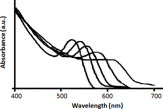
A typical absorption spectrum of narrow size distribution wurtzite CdSe quantum dot is shown in [link] . A size evolving absorption spectra is shown in [link] . However, a complete analysis of the sample is possible only by also studying the fluorescence properties of CdSe.


Cadmium telluride has a band gap of 1.44 eV (860 nm) and as such it absorbs in the infrared region. Like CdSe, the sizes of CdTe can be engineered to have different band edges and thus, different absorption spectra as a function of wavelength. A typical CdTe spectra is shown in [link] . Due to the small bandgap energy of CdTe, it can be used in tandem with CdSe to absorb in a greater part of the solar spectrum.
[link] shows the bulk band gap of other Group 12-16 semiconductor systems. The band gap of ZnS falls in the UV region, while those of ZnSe, CdS, and ZnTe fall in the visible region.
| Material | Band gap (eV) | Wavelength (nm) |
| ZnS | 3.61 | 343.2 |
| ZnSe | 2.69 | 460.5 |
| ZnTe | 2.39 | 518.4 |
| CdS | 2.49 | 497.5 |
| CdSe | 1.74 | 712.1 |
| CdTe | 1.44 | 860.3 |
It is often desirable to have a combination of two Group 12-16 semiconductor system quantum heterostructures of different shapes like dots and tetrapods, for applications in solar cells, bio-markers, etc. Some of the most interesting systems are ZnS shell-CdSe core systems, such as the CdSe/CdS rods and tetrapods.
[link] shows a typical absorption spectra of CdSe-ZnS core-shell system. This system is important because of the drastically improved fluorescence properties because of the addition of a wide band gap ZnS shell than the core CdSe. In addition with a ZnS shell, CdSe becomes bio-compatible.

A CdSe seed, CdS arm nanorods system is also interesting. Combining CdSe and CdS in a single nanostructure creates a material with a mixed dimensionality where holes are confined to CdSe while electrons can move freely between CdSe and CdS phases.
Notification Switch
Would you like to follow the 'Nanomaterials and nanotechnology' conversation and receive update notifications?

|
|

|
|

|
|

|
|

|
|

|
|
|
|

|
|

|
|

|