

| << Chapter < Page | Chapter >> Page > |
A semiconductor is a material that has unique properties in the way it reacts to electrical current. A semiconductor’s ability to conduct an electrical current is intermediate between that of an insulator (such as rubber or glass) and a conductor (such as copper). However, the conductivity of a semiconductor material increases with increasing temperature, a behavior opposite to that of a metal. Semiconductors may also have a lower resistance to the flow of current in one direction than in the other.
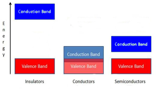
The properties of semiconductors can best be understood by band theory, where the difference between conductors, semiconductors, and insulators can be understood by increasing separations between a valence band and a conduction band , as shown in [link] . In semiconductors a small energy gap separates the valence band and the conduction band. This energy gap is smaller than that of insulators – which is too large for essentially any electrons from the valence band to enter the conduction band – and larger than that of conductors, where the valence and conduction bands overlap. At 0 K all of the electrons in a semiconductor lie in the valence band, but at higher temperatures some electrons will have enough energy to be promoted to the conduction band
In addition to the band structure of solids, the concept of carrier generation and recombination is very important to the understanding of semiconducting materials. Carrier generation and recombination is the process by which mobile charge carriers (electrons and electron holes) are created and eliminated. The valence band in semiconductors is normally very full and its electrons immobile, resulting in no flow as electrical current. However, if an electron in the valence band acquires enough energy to reach the conduction band, it can flow freely in the nearly empty conduction band. Furthermore, it will leave behind an electron hole that can flow as current exactly like a physical charged particle. The energy of an electron-electron hole pair is quantified in the form of a neutrally-charged quasiparticle called an exciton. For semiconducting materials, there is a characteristic separation distance between the electron and the hole in an exciton called the exciton Bohr radius. The exciton Bohr radius has large implications for the properties of quantum dots.
The process by which electrons gain energy and move from the valence to the conduction band is termed carrier generation, while recombination describes the process by which electrons lose energy and re-occupy the energy state of an electron hole in the valence band. Carrier generation is accompanied by the absorption of radiation, while recombination is accompanied by the emission of radiation.
In the 1980s, a new nanoscale (~1-10 nm) semiconducting structure was developed that exhibits properties intermediate between bulk semiconductors and discrete molecules. These semiconducting nanocrystals, called quantum dots, are small enough to be subjected to quantum effects, which gives them interesting properties and the potential to be useful in a wide-variety of applications. The most important characteristic of quantum dots (QDs) is that they are highly tunable, meaning that the optoelectronic properties are dependent on the particles size and shape. As [link] illustrates, the band gap in a QD is inversely related to its size, which produces a blue shift in emitted light as the particle size decreases. The highly tunable nature of QDs result not only from the inverse relationship between band gap size and particle size, but also from the ability to set the size of QDs and make QDs out of a wide variety of materials. The potential to produce QDs with properties tailored to fulfill a specific function has produce an enormous amount of interest in quantum dots (see Optical Properties of Group 12-16 (II-VI) Semiconductor Nanoparticles ).
Notification Switch
Would you like to follow the 'Nanomaterials and nanotechnology' conversation and receive update notifications?

|
|

|
|

|
|

|
|

|
|

|
|
|
|
|

|
|
|
|
|

|