

| << Chapter < Page | Chapter >> Page > |
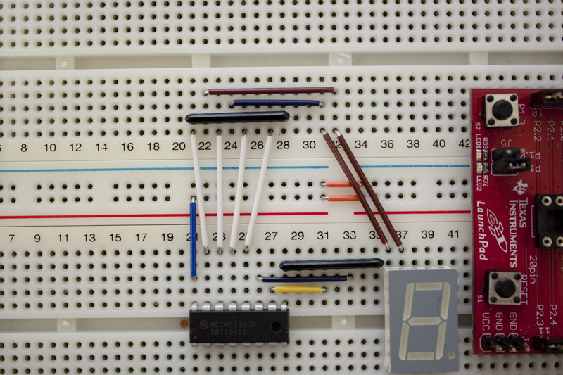
Connect the first four outputs of the decoder to the upper resistor array. Decoder pins 12-15 (lower A-E columns 22-25) fan out to every other pin in the upper array (upper F-J columns 21, 23, 25, 27) (white wires in image below).
The lower resistor array already has one connection made for us (the decoder pin 9 and pin 1 of the resistor array share the same column). Run a wire from decoder pin 10 (lower A-E column 27) to resistor array pin 4 (lower A-E column 31). Then connect decoder pin 11 (lower A-E column 26) to resistor pin 6 (lower A-E column 37).

Since this is the most complicated step, it is broken down into individual sub-steps. Each picture shows one additional route, eventually connecting all of the resistor array outputs to their respective display inputs. If you prefer to work on the circuit as one block and would like to see the end result, just skip ahead to step 10.
Connect the upper resistor pack pin 4 (upper F-J column 24) to column 31. Then connect column 31 to display pin 10 (lower A-E column 36).

Connect the upper resistor pack pin 2 (upper F-J column 22) to column 32. Then connect column 32 to display pin 9 (lower A-E column 37).
Connect the upper resistor pack pin 6 (upper F-J column 26) to column 34. Then connect column 34 to display pin 7 (lower A-E column 39).

Connect the upper resistor pack pin 8 (upper F-J column 28) to column 35. Then connect column 35 to display pin 6 (lower A-E column 40).

Now start working with the bottom resistor array. Jump the lower resistor pack pin 2 (lower A-E column 29) to column 29 F-J on the other side of the channel. Then connect lower F-J column 29 to display pin 1 (lower F-J column 36).

Again, jump the lower resistor pack pin 3 (lower A-E column 30) to column 30 F-J on the other side of the channel. Then connect lower F-J column 30 to display pin 2 (lower F-J column 37).

Finally, jump the lower resistor pack pin 5 (lower A-E column 32) to column 32 F-J on the other side of the channel. Then connect lower F-J column 32 to display pin 4 (lower F-J column 39).

Start with the longest runs from GPIO pins P1.4 and P1.5 on the MSP430 Launchpad (breadboard channels 50 and 51). Use a long yellow wire to go from GPIO P1.4 (upper A-E channel 51) to decoder pin 7 (lower F-J channel 27) . Then use a long green wire to go from GPIO P1.5 (upper A-E channel 50) to decoder pin 1 (lower F-J channel 21) .
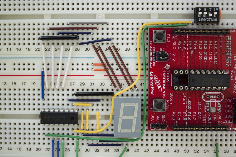


Now use two of the long orange wires to connect GPIO 1.7 (lower F-J column 51) to decoder pin 6 (lower F-J column 26) and GPIO 1.6 (lower F-J column 50) to decoder pin 2 (lower F-J column 22). Be careful not to accidentally cross the connections! See below for one way to bed the wires so they fit the length of the wire run.


Now that you've completed your breadboard, you are ready to begin! It is strongly recommended that you run the provided test program to make sure all of you connections have been made correctly. Knowing that there are no issues with your underlying hardware will make troubleshooting down the road much less frustrating.

Notification Switch
Would you like to follow the 'Intro to computational engineering: elec 220 labs' conversation and receive update notifications?

|
|

|
|

|
|

|
|

|
|

|
|

|
|

|
|

|
|

|